


8XC251SA, SB, SP, SQ USER’S MANUAL
A-58
Example: The on-chip RAM locations 40H, 50H, and 60H contain 01H, 70H, and 15H, respectively.
After executing the following instruction sequence
DJNZ 40H,LABEL1
DJNZ 50H,LABEL2
DJNZ 60H,LABEL
on-chip RAM locations 40H, 50H, and 60H contain 00H, 6FH, and 14H, respectively, and
program execution continues at label LABEL2. (The first jump was not taken because the
result was zero.)
This instruction provides a simple way of executing a program loop a given number of times,
or for adding a moderate time delay (from 2 to 512 machine cycles) with a single instruction.
The instruction sequence,
toggles P1.7 eight times, causing four output pulses to appear at bit 7 of output Port 1. Each
pulse lasts three states: two for DJNZ and one to alter the pin.
Variations
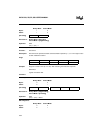
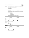
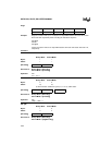
DJNZ dir8,rel
Binary Mode Source Mode
Not Taken Taken Not Taken Taken
Bytes: 33 33
States: 36 36
Hex Code in: Binary Mode = [Encoding]
Source Mode = [Encoding]
Operation: DJNZ
(PC) ← (PC) + 2
(dir8) ← (dir8) – 1
IF (dir8) > 0 or (dir8) < 0
THEN
(PC) ← (PC) + rel
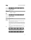
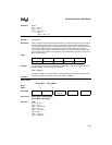
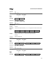
DJNZ Rn,rel
Binary Mode Source Mode
Not Taken Taken Not Taken Taken
Bytes: 22 33
States: 2 5 3 6
Hex Code in: Binary Mode = [Encoding]
Source Mode = [A5][Encoding]
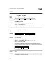
TOGGLE:
MOV R2,#8
CPL P1.7
DJNZ R2,TOGGLE
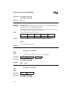
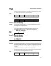
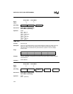
[Encoding] 1 1 0 1 0 1 0 1 direct addr rel. addr
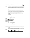
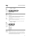
[Encoding] 1 1 0 1 1 r r r rel. addr