


13-3
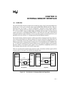
EXTERNAL MEMORY INTERFACE
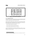
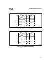
13.2 EXTERNAL BUS CYCLES
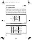
The section describes the bus cycles the 8XC251Sx executes to fetch code, read data, and write
data in external memory. Both page mode and nonpage mode are described and illustrated. For
simplicity, the accompanying figures depict the bus cycle waveforms in idealized form and do not
provide precise timing information. This section does not cover wait states (see section 13.4, “Ex-
ternal Bus Cycles with Configurable Wait States”) or configuration byte bus cycles (see section
13.6, “Configuration Byte Bus Cycles”). For bus cycle timing parameters refer to the datasheet.
An “inactive external bus” exists when the 8XC251Sx is not executing external bus cycles. This
occurs under any of the three following conditions:
• Bus Idle (The chip is in normal operating mode but no external bus cycles are executing)
• The chip is in idle mode
• The chip is in powerdown mode
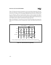
13.2.1 Bus Cycle Definitions
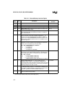
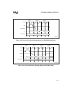
Table 13-2 lists the types of external bus cycles. It also shows the activity on the bus for nonpage
mode and page mode bus cycles with no wait states. There are three types of nonpage mode bus
cycles: code read, data read, and data write. There are four types of page mode bus cycles: code
fetch (page miss), code read (page hit), data read, and data write. The data read and data write
cycles are the same for page mode and nonpage mode (except the multiplexing of D7:0 on ports
0 and 2).
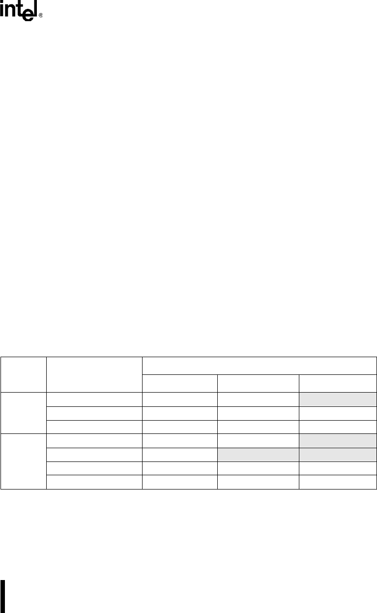
Table 13-2. Bus Cycle Definitions (No Wait States)
Mode Bus Cycle
Bus Activity
State 1 State 2 State 3
Nonpage
Mode
Code Read ALE RD#/PSEN#, code in
Data Read (2) ALE RD#/PSEN# data in
Data Write (2) ALE WR# WR# high, data out
Page
Mode
Code Read, Page Miss ALE RD#/PSEN#, code in
Code Read, Page Hit (3) PSEN#, code in
Data Read (2) ALE RD#/PSEN# data in
Data Write (2) ALE WR# WR# high, data out
NOTES:
1. Signal timing implied by this table is approximate (idealized).
2. Data read (page mode) = data read (nonpage mode) and write (page mode) = write (nonpage mode)
except that in page mode data appears on P2 (multiplexed with A15:0), whereas in nonpage mode
data appears on P0 (multiplexed with A7:0).
3. The initial code read page hit bus cycle can execute only following a code read page miss cycle.