14-1
CHAPTER 14
PROGRAMMING AND VERIFYING
NONVOLATILE MEMORY
This chapter provides instructions for programming and verifying on-chip nonvolatile memory
on the 8XC251Sx. The programming instructions cover the entry of program code into on-chip
code memory, configuration information into the on-chip configuration bytes, and other catego-
ries of information into on-chip memory outside the memory address space. The verify instruc-
tions permit reading these memory locations to verify their contents. The operations covered in
this chapter are:
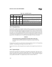
• programming and verifying the on-chip code memory (8 Kbytes, 16 Kbytes)
• programming and verifying the on-chip configuration bytes (8 bytes)
• programming and verifying the lock bits (3 bits)
• programming the encryption array (128 bytes)
• verifying the signature bytes (3 bytes)
Programming instructions apply to the 87C251Sx (one-time programmable ROM (OTPROM)
and erasable programmable ROM (EPROM)). Verify instructions apply to the 87C251Sx, the
83C251Sx (mask ROM), and the configuration bytes on the 80C251SB, SQ (no ROM/OTPROM/
EPROM). In the unprogrammed state, EPROM and OTPROM contains all 1s.
14.1 GENERAL
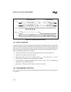
The 87C251Sx is programmed and verified in the same manner as the 87C51FX, using the same
quick-pulse programming algorithm, which programs at V
PP
= 12.75 V using a series of five
100-µs PROG# pulses per byte. This results in a programming time of approximately 16 seconds
for the 16-Kbyte on-chip code memory.
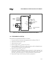
Programming and verifying operations differ from normal microcontroller operation. Memory
accesses are made one byte at a time, input/output ports are used in a different manner, and the
EA#/V
PP
and ALE/PROG# pins are used for their alternative (programming) functions. For a
complete list of signal descriptions, see Appendix B.


