5
5
4
4
3
3
2
2
1
1
D D
C C
B B
A A
No license, express or implied, by estoppel or otherwise, to any
intellectual property rights is granted herein.
Revision
A1
THIS DRAWING CONTAINS INFORMATION WHICH HAS NOT
BEEN VERIFIED FOR MANUFACTURING AS AN END USER
PRODUCT. INTEL IS NOT RESPONSIBLE FOR THE
MISUSE OF THIS INFORMATION.
Intel disclaims all liability, including liability for
infringement of any proprietary rights, relating to use of
information in this specification. Intel does not warrant or
represent that such use will not infringe such rights.
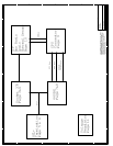
History
REV A0 to REV A1 Changes
1. Removed Translator logic for
PREQ0#
2. Removed Termination Resistors on
BX side for GTL+
3. Added 20pF load on HCLK for BX
clock compensating
Celeron(TM) Processor
in PPGA Daughter Board
THIS SCHEMATIC IS PROVIDED "AS IS" WITH NO WARRANTIES
WHATSOEVER, INCLUDING ANY WARRANTY OF MERCHANTABILITY,
FITNESS FOR ANY PARTICULAR PURPOSE, OR ANY WARRANTY
OTHERWISE ARISING OUT OF PROPOSAL, SPECIFICATION OR
SAMPLE.
Celeron Processor Adaptor A
Title Page / Revision
Embedded Microcontroller Division (EMD)
Intel Corporation
5000 W. Chandler Blvd
Chandler AZ, 85044
C
111Tuesday, May 11, 1999
Title
Size Document Number Rev
Date: Sheet of


