


iv
Celeron™ Processor Development Kit Manual
3.2.19 Post Code Debugger.........................................................................3-6
3.2.20 Clock Generation...............................................................................3-6
3.2.21 Interrupt Map.....................................................................................3-6
3.2.22 Memory Map .....................................................................................3-7
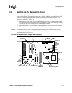
4 Hardware Reference ..............................................................................................4-1
4.1 Processor Assembly ..........................................................................................4-1
4.1.1 Thermal Management .......................................................................4-1
4.1.2 ITP Debugger Port ............................................................................4-1
4.2 Post Code Debugger..........................................................................................4-1
4.3 ISA and PCI Expansion Slots.............................................................................4-2
4.4 PCI Device Mapping ..........................................................................................4-2
4.5 Connector Pinouts..............................................................................................4-3
4.5.1 ATX Power Connector.......................................................................4-3
4.5.2 ITP Debugger Connector ..................................................................4-4
4.5.3 Stacked USB.....................................................................................4-4
4.5.4 Mouse and Keyboard Connectors.....................................................4-5
4.5.5 Parallel Port.......................................................................................4-5
4.5.6 Serial Ports........................................................................................4-6
4.5.7 IDE Connector...................................................................................4-6
4.5.8 Floppy Drive Connector.....................................................................4-7
4.5.9 PCI Slot Connector............................................................................4-8
4.5.10 ISA Slot Connector............................................................................4-9
4.6 AGP Connector................................................................................................4-10
4.7 Jumpers ...........................................................................................................4-11
4.7.1 Enable Spread Spectrum Clocking (J14) ........................................4-11
4.7.2 Clock Frequency Selection (J15) ....................................................4-11
4.7.3 On/Off (J20).....................................................................................4-11
4.7.4 Flash BIOS VPP Select (J21)..........................................................4-12
4.7.5 Flash BIOS Boot Block Control (J22)..............................................4-12
4.7.6 SMI# Source Control (J23)..............................................................4-12
4.7.7 CMOS RAM Clear (J24)..................................................................4-12
4.7.8 Push Button Switches .....................................................................4-12
4.8 In-Circuit BIOS Update.....................................................................................4-13
5 BIOS Quick Reference ..........................................................................................5-1
5.1 BIOS and Pre-Boot Features .............................................................................5-1
5.2 Power-On Self-Test (POST) ..............................................................................5-1
5.3 Setup Screen System ........................................................................................5-3
5.3.1 Basic CMOS Configuration Screen ...................................................5-3
5.3.2 Configuring Drive Assignments.........................................................5-4
5.3.2.1 Configuring Floppy Drive Types ..........................................5-4
5.3.3 Configuring IDE Drive Types.............................................................5-5
5.4 Configuring Boot Actions....................................................................................5-6
5.5 Custom Configuration Setup Screen..................................................................5-6
5.6 Shadow Configuration Setup Screen .................................................................5-7
5.7 Standard Diagnostics Routines Setup Screen ...................................................5-8
5.8 Start System BIOS Debugger Setup Screen .....................................................5-8
5.9 Start RS232 Manufacturing Link Setup Screen .................................................5-9
5.10 Manufacturing Mode ..........................................................................................5-9