


A
A
B
B
C
C
D
D
E
E
4 4
3 3
2 2
1 1
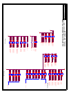
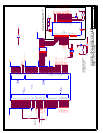
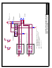
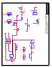
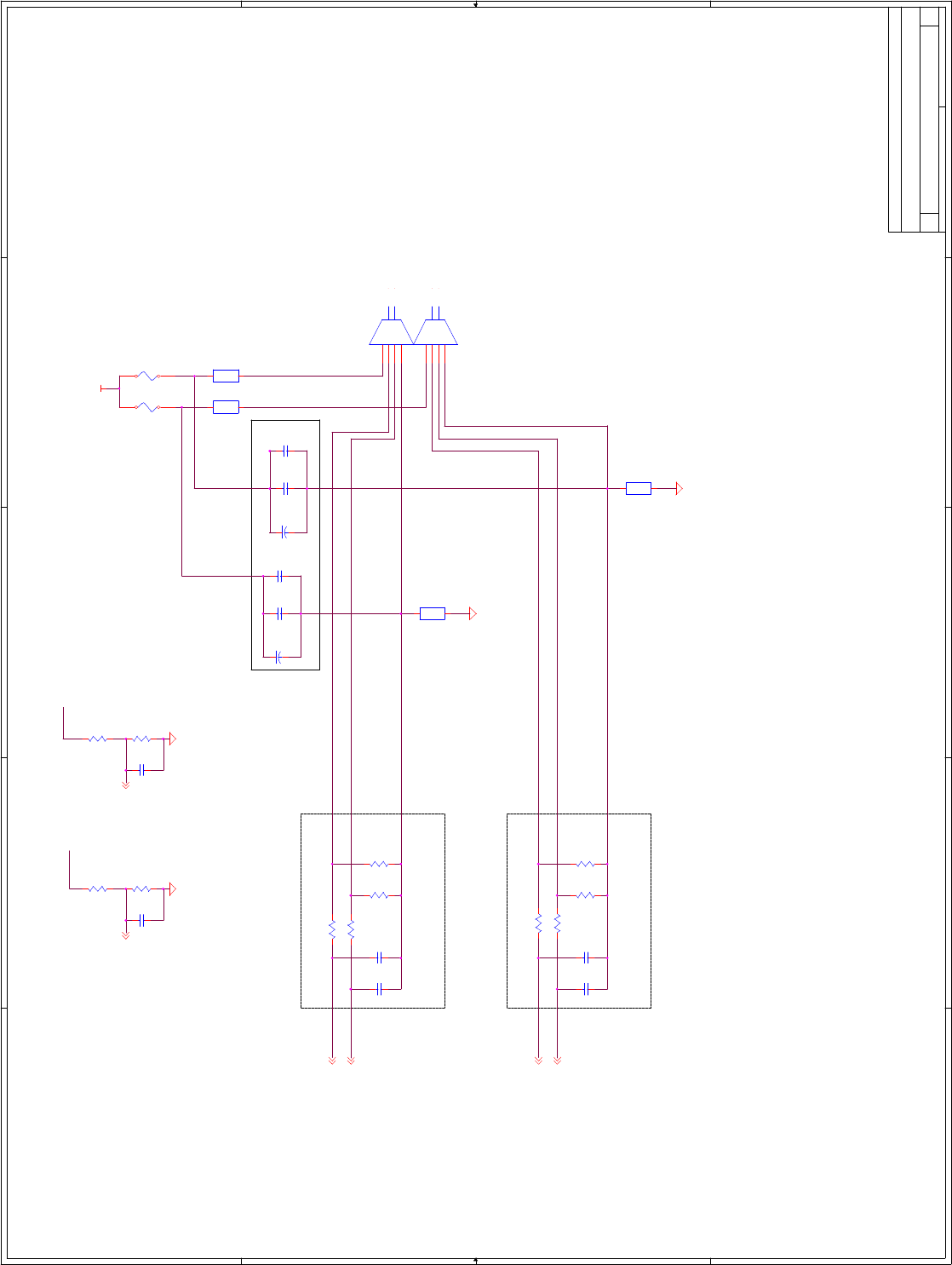
NOTE 1: USB differential traces route together (Z0- & Z0+) and (Z1- & Z1+).
Must be 45 Ohm Matched
Stripline width 0.015 (for 1 oz)->44.88/45.45 Ohm.
8Ohm/100MHz/500mA
8Ohm/100MHz/500mA
PCB Trace 45 Ohm Matched, Routed Together
Stripline width 0.015 (1 oz) 44.88/45.45
Ohm
Poly-Fuse Poly-Fuse
NOTE 2: Protect differential traces w/ guard traces or
double space to any other signal.
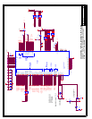
Place As Close as
Possible to PIIX4
Place As Close as
Possible to PIIX4
PCB Trace 45 Ohm Matched,
Routed Together
Stripline width 0.015 (1 oz)
44.88/45.45 Ohm
NOTE 3: Place ferrites at connector.
NOTE 4: Poly-fuse min 1.5A
max 5A.
BOTTOM of Stacked
USB Connector
TOP of Stacked
USB Connector
Poly fuses should be in range
of 1.5A to 5A
Place these caps within 1 inch
of USB Connector stack
THIS DRAWING CONTAINS INFORMATION WHICH HAS NOT
BEEN VERIFIED FOR MANUFACTURING AS AN END USER
PRODUCT. INTEL IS NOT RESPONSIBLE FOR THE
MISUSE OF THIS INFORMATION.
{Doc}
D
USB Connectors
C
17 22Thursday, February 25, 1999
Title
Size Document Number Rev
Date: Sheet of
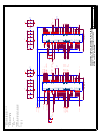
Z1_VCC Z0_VCC
Z1_GND
Z0+
Z1-
Z1+
Z0-
USBVFIL1
USBVFIL2
USBVFIL1
USBVFIL2
Z0_GND
USBP1-14
USBP1+14
OC0#14OC1#14
USBP0+14
USBP0-14
V5_0
FB3
BLM41A800S
1 2
1 2
F2
SMD250-002
FB4
BLM41A800S
1 2
1 2
J2
USB Stack
1
2
3
4
5
6
7
8
9
10
11
12
VCC0
D0-
D0+
GND0
VCC1
D1-
D1+
GND1
GND
GND
GND
GND
FB1
BLM41A800S
12
12
FB2
BLM41A800S
12
12
F1
SMD250002
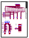
C158
0.01uF
C157
0.1uF
C23
0.01uF
C22
0.1uF
C125
47pF
C124
47pF
C1
0.01UF
C7
0.01UF
R93
27
R90
15K
R94
27
R88
15K
R91
15K
R89
15K
R92
27
R4
10K
R3
15K
R2
10K
R1
15K
C2
100uF
C6
100uF
C123
47pF
R95
27
C122
47pF