


3-6
Celeron™ Processor Development Kit Manual
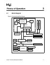
Theory of Operation
3.2.19 Post Code Debugger
The evaluation board has an on-board Post Code Debugger. Data from any program that does an
I/O write to 0080H is latched and displayed on the two LEDs (U12 and U13). During BIOS startup,
codes are posted to these LEDs to indicate what the BIOS is doing. Application programs can post
their own data to these LEDs by writing to I/O address 0080H.
3.2.20 Clock Generation
There are three devices on the baseboard which generate and distribute the clocks used by the
entire system. These are the CY2280 clock synthesizer, CY2318NZ clock buffer and the CY23009
zero delay buffer. Not all of these devices are used on this version of the evaluation board.
The CY2280 generates the clocks for the Celeron processor, Host Bridge/Controller, cache, PCI,
USB and ISA bus. The processor clock runs at 66 MHz. The PCI clocks run at 33 MHz. This
device is capable of spread spectrum clocking. If spread spectrum clocking is enabled, a 0.5%
down spread will be introduced in the processor and PCI clocks.
The CY2318NZ clock buffer is used to buffer the clock signals sent to the SDRAM DIMMS. The
SDRAM interface operates at 66 MHz.
The CY2309 Zero Delay Buffer is not used by the evaluation board.
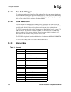
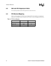
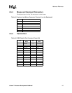
3.2.21 Interrupt Map
Table 3-1. Interrupts
IRQ System Resources
NMI I/O Channel Check
0 Reserved, Interval Timer
1 Reserved, Keyboard buffer full
2 Reserved, Cascade interrupt from slave PIC
3 Serial Port 2
4 Serial Port 1
5 Parallel Port (PNP0 option)
6 Floppy
7 Parallel Port 1
8 Real Time Clock
9 IRQ2 Redirect
10 Reserved. Not supported.
11 Reserved. Not supported.
12 Onboard Mouse Port if present, else user available
13 Reserved, Math coprocessor
14 Primary IDE if present, else user available
15 Reserved. Not supported.