


Celeron™ Processor Development Kit Manual
4-1
Hardware Reference
4
This section provides reference information on the system design. Included in this section is
connector pinout information, jumper settings, and other system design information.
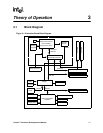
4.1 Processor Assembly
The processor assembly contains the Celeron™ processor, the 82443BX Host Bridge/Controller, a
voltage regulator and an ITP debugger connector. The assembly connects to the baseboard via a
400-pin connector.
Warning: The processor assembly is attached to the baseboard at the factory. Do not remove the processor
assembly from the baseboard. Intel will not support the processor assembly or the baseboard if any
portion of the assembly is removed by the customer.
4.1.1 Thermal Management
The objective of thermal management is to ensure that the temperature of each component is
maintained within specified functional limits. The functional temperature limit is the range within
which the electrical circuits can be expected to meet their specified performance requirements.
Operation outside the functional limit can degrade system performance and cause reliability
problems.
Important: The evaluation kit contains a heatsink and fan attached to the top of the Celeron processor. This
thermal solution has been tested in an open air environment at room temperature and is sufficient
for evaluation purposes only. It is up to the designer to provide adequate thermal management for
any designs derived from the schematics provided in your kit.
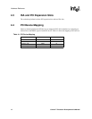
4.1.2 ITP Debugger Port
The evaluation platform is populated with a 2.5 V ITP debugger port. The ITP port provides a path
for debugger tools like emulators, in-target probes, and logic analyzers to gain access to the
Celeron processor’s registers and signals without affecting high speed operation. This allows the
system to operate at full speed with the debugger attached.
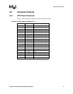
4.2 Post Code Debugger
The evaluation board has an on-board Post Code Debugger. Data from any code that does an I/O
write to 80H is latched on the two led displays (U12/U13). During BIOS startup, code is posted to
these LEDs to indicate what the BIOS is doing. Application code can post its own data to these
LEDs by doing an I/O write to address 80H. The 22V10 PLD code used to implement this function
is included in Appendix A, “PLD Code Listing.”