


Theory of Operation
6–8
760A / 760D / 760N
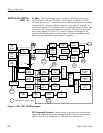
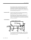
U5 pin 2 is the inverting input of an internal op-amp. The noninverting input is
set to 2.5 V by an internal voltage reference. Current from the peak detector
flows through R83 and R79. R84 provides a 100 mA offset. The voltage at U5
pin 1 will vary in order to maintain U5 pin 2 at 2.5 V.
The voltage at U5 pin 1 is modified by an internal circuit and sets the trip point
of the internal comparator. U5 pin 3 is the external input to the comparator. R88
and C52, connected to U5 pin 4, set the internal oscillator to 80 kHz.
The circuit works as follows: The oscillator resets the latch and U5 pin 6 goes
high, turning the switcher mosfet on. The current through the switcher mosfet
increases, causing the voltage across R96 to increase. This voltage is divided by
R87 and R101, and is applied to the comparator (pin 3). When the voltage at U5
pin 3 reaches the comparator trip point, the latch toggles and the switcher mosfet
is turned off. This process is repeated at an 80 kHz rate.
C58 increases the PWM noise immunity by rolling off the internal op-amp
frequency response. R82 holds the switcher mosfet off as the circuit is powering
up. R81 slows the turn-on of the switcher mosfet while CR27 speeds up the
turn–off.
The three output windings supply four output voltages. Each output is rectified
by a single diode and filtered by an LC pi filter.
The Error Amplifier regulates the +5 V output by feeding an error signal to the
Pulse Width Modulator. VR1 is a 2.5 V shunt regulator containing an op-amp
and a voltage reference. The +5 V is divided by R69 and R70 to provide 2.5 V
to VR1, with fine adjustment provided by R99. C40 and R71 determine the gain
and frequency response of VR1. VR4 controls overshoot of the +5 V at power
up. R98 and CR26 provide a minimum operating current for VR1. R68
decouples C39 from VR1. Overvoltage protection for the +5V supply is
provided by a crowbar circuit formed by Q11, VR3, R13, and R14.
The 80 kHz sawtooth waveform at U3 pin 3 trips comparator U3. U3 pin 1 then
feeds a trigger pulse to one-shot U4. U4 pin 13 outputs a 300 ns pulse to the
130 mA current source consisting of Q7 and Q8. When Q8 turns on, T2 pin 2 is
pulled down until CR15 (Error Amplifier) is forward biased. The negative-going
pulse at T2 pin 2 is peak detected by CR16 and C46. The DC voltage present at
the anode of CR16 feeds the pulse width modulator and the Output Under-Volt-
age Shutdown circuit. CR29 resets T2 between pulses.
If the +5 V is below 4.9 V, the Error Amplifier will cause the Peak Detector
output to go below 2.9 V. The output of comparator U3B will pull low and shut
down pulse width modulator U5. C47 and R96 delay the operation of U3B long
enough for the power supply to power up. If the +5 V does not reach 4.9 V
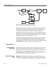
Output Filters
Error Amplifier
Feedback Transformer
Driver and Peak Detector
Output Under-Voltage
Shutdown