2-7
ARCHITECTURAL OVERVIEW
2.4 INTERNAL TIMING
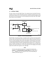
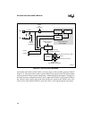
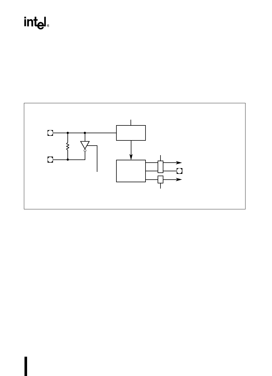
The clock circuitry of the 8XC196NP (Figure 2-3) is identical to that of earlier MCS 96 micro-
controllers. It receives an input clock signal on XTAL1 provided by an external crystal or clock
and divides the frequency by two. The clock generators accept the divided input frequency from
the divide-by-two circuit and produce two nonoverlapping internal timing signals, PH1 and PH2.
These signals are active when high.
Figure 2-3. Clock Circuitry (8XC196NP)
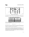
The 80C196NU’s clock circuitry (Figure 2-4) implements phase-locked loop and clock multiplier
circuitry, which can substantially increase the CPU clock rate while using a lower-frequency in-
put clock. The clock circuitry accepts an input clock signal on XTAL1 provided by an external
crystal or oscillator. Depending on the values of the PLLEN1 and PLLEN2 pins, this frequency
is routed either through the phase-locked loop and multiplier or directly to the divide-by-two cir-
cuit. The multiplier circuitry can double or quadruple the input frequency (F
XTAL1
) before the fre-
quency (f) reaches the divide-by-two circuitry. The clock generators accept the divided input
frequency (f/2) from the divide-by-two circuit and produce two nonoverlapping internal timing
signals, PH1 and PH2. These signals are active when high.
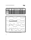
NOTE
For brevity, this manual uses lowercase “f” to represent the internal clock
frequency of both the 8XC196NP and the 80C196NU. For the 8XC196NP, f is
equal to F
XTAL1
. For the 80C196NU, f is equal to either F
XTAL1
, 2F
XTAL1
, or
4F
XTAL1
, depending on the clock multiplier mode, which is controlled by the
PLLEN1 and PLLEN2 input pins.
A3161-01
Clock
Generators
CPU Clocks (PH1, PH2)
Divide-by-two
Circuit
Peripheral Clocks (PH1, PH2)
CLKOUT
Disable Clocks
(Powerdown)
Disable Clocks
(Idle, Powerdown)
XTAL1
XTAL2
Disable
Oscillator
(Powerdown)
Disable Clock Input
(Powerdown)
F
XTAL1


