8XC196NP, 80C196NU USER’S MANUAL
13-20
A design can incorporate external devices that operate with different bus widths and multiplex-
ing. The bus parameters used during a particular bus cycle are determined by the chip-select out-
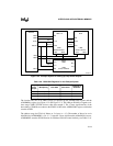
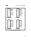
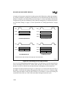
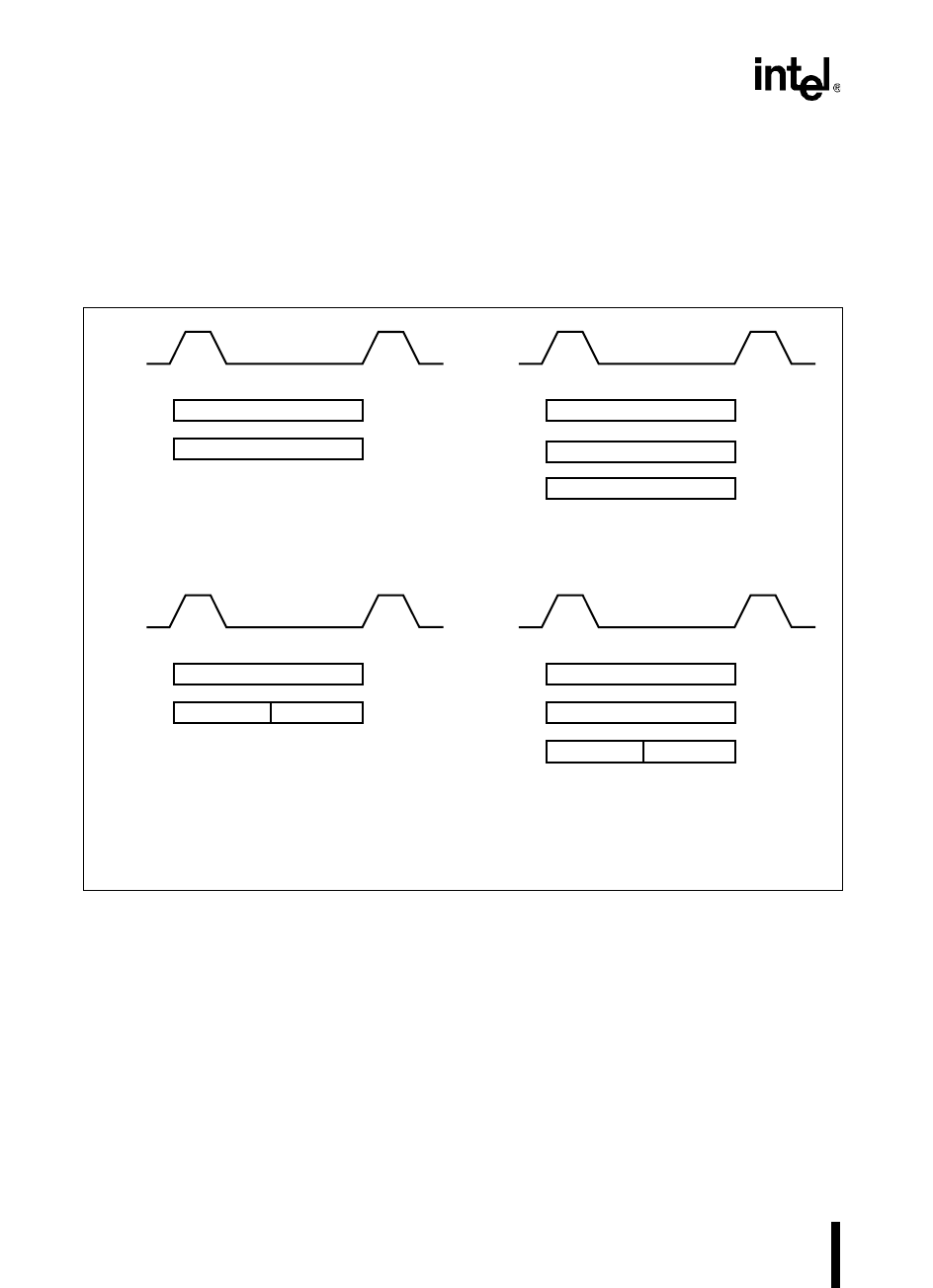
put that is assigned to the address being accessed. Figure 13-9 shows the address and data bus
configurations for the four combinations of bus width and multiplexing. For detailed waveforms,
see “16-bit Bus Timings” on page 13-22 and “System Bus AC Timing Specifications” on page
13-36.
Figure 13-9. Bus Activity for Four Types of Buses
In an 8- or 16-bit demultiplexed mode (top of Figure 13-8 and Figure 13-9), the external device
receives the address from A19:0. In a 16-bit system, the data is on AD15:0. In an 8-bit system,
the data is on AD7:0. AD15:8 drive the data currently on the high byte of the internal bus.
In multiplexed mode (bottom half of Figure 13-8 and Figure 13-9), both A19:0 and AD15:0 drive
the address. A19:0 drive the address throughout the entire bus cycle. For a 16-bit bus width,
AD15:0 drive the address for the first half of the bus cycle and drive or receive data during the
second half. In the 8-bit case, AD15:8 drive the address during the entire bus cycle.
ALE
A2463-02
ALE
A19:0 Address
AD15:0 Data
A19:0 Address
AD7:0 Data
16-bit Demultiplexed Bus 8-bit Demultiplexed Bus
ALE
ALE
A19:0 Address
AD15:0 Data
A19:0 Address
AD15:8 Address
AD7:0
16-bit Multiplexed Bus 8-bit Multiplexed Bus
Address
Data
Address
AD15:8
Driven†
† AD15:8 drive the data currently on the high byte of the internal bus.


