8XC196NP, 80C196NU USER’S MANUAL
13-34
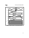
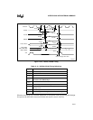
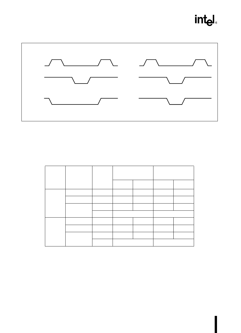
Figure 13-17. Write-control Signal Waveforms
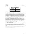
Table 13-14 compares the values of the write-control signals for write operations in the standard
mode and the write strobe mode. The table lists values of WR# and BHE# and values of WRL#
and WRH# for 8-bit and 16-bit writes on an 8-bit and 16-bit bus.
To select the standard write-control mode, set CCR0.2. In standard mode, the WR#/WRL# pin
operates as WR#, and the BHE#/WRH# pin operates as BHE#. WR# is asserted for every external
memory write. BHE# is asserted for word accesses (read and write) and for byte accesses to odd
addresses. BHE# can be used to select the bank of memory that stores the high (odd) byte. Figure
13-10 on page 13-22 illustrates use of the standard mode in a 16-bit system. In this example, WR#
writes words to the 16-bit flash memory. To write individual bytes, you can use the decoding logic
in Figure 13-18 or use the write strobe mode.
Table 13-14. Write Signals for Standard and Write Strobe Modes
Bus
Width
Word/Byte
Written
A0
Standard
(CCR0.2 = 1)
Write Strobe
(CCR0.2 = 0)
WR# BHE# WRL# WRH#
8
Low Byte00100
High Byte 1 0 0 0 0
Word
00000
1 Illegal Illegal
16
Low Byte00101
High Byte 1 0 0 1 0
Word
00000
1 Illegal Illegal
A2472-02
ALE
WR#
BHE#
ALE
WRL#
WRH#
Standard Mode Write Strobe Mode
Active for low- or high-byte write. Active for low-byte write.
Active for high-byte write. Active for high-byte write.


