8XC196NP, 80C196NU USER’S MANUAL
B-10
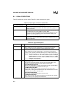
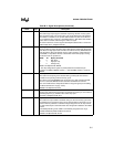
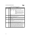
PLLEN2:1
(NU only)
I Phase-locked Loop 1 and 2 Enable
These input pins are used to enable the on-chip clock multiplier feature and
select either the doubled or quadrupled clock speed as follows:
PLLEN1 PLLEN2 Mode
0 0 standard mode; clock multiplier circuitry disabled.
Internal clock equals the XTAL1 input frequency.
0 1 Reserved
†
1 0 doubled mode; clock multiplier circuitry enabled.
Internal clock is twice the XTAL1 input frequency.
1 1 quadrupled mode; clock multiplier circuitry enabled.
Internal clock is four times the XTAL1 input
frequency.
†
This reserved combination causes the device to enter an unsupported test
mode.
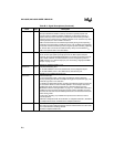
PWM2:0 O Pulse Width Modulator Outputs
These are PWM output pins with high-current drive capability. The duty cycle
and frequency-pulse-widths are programmable.
PWM2:0 are multiplexed with P4.2:0.
RD# O Read
Read-signal output to external memory. RD# is asserted only during external
memory reads.
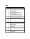
READY I Ready Input
This active-high input signal is used to lengthen external memory cycles for
slow memory by generating wait states in addition to the wait states that are
generated internally.
When READY is high, CPU operation continues in a normal manner with wait
states inserted as programmed in CCR0 or the chip-select
x
bus control
register. READY is ignored for all internal memory accesses.
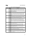
RESET# I/O Reset
A level-sensitive reset input to and open-drain system reset output from the
microcontroller. Either a falling edge on RESET# or an internal reset turns on a
pull-down transistor connected to the RESET# pin for 16 state times. In the
powerdown, standby, and idle modes, asserting RESET# causes the chip to
reset and return to normal operating mode. After a device reset, the first
instruction fetch is from FF2080H (or F2080H in external memory). For the
80C196NP and 80C196NU, the program and special-purpose memory
locations (FF2000–FF2FFFH) reside in external memory. For the 83C196NP,
these locations can reside either in external memory or in internal ROM.
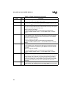
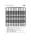
Table B-3. Signal Descriptions (Continued)
Name Type Description


