8XC196NP, 80C196NU USER’S MANUAL
2-2
2.2 DEVICE FEATURES
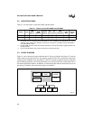
Table 2-1 lists the features of the 8XC196NP and 80C196NU.
2.3 BLOCK DIAGRAM
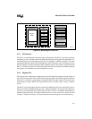
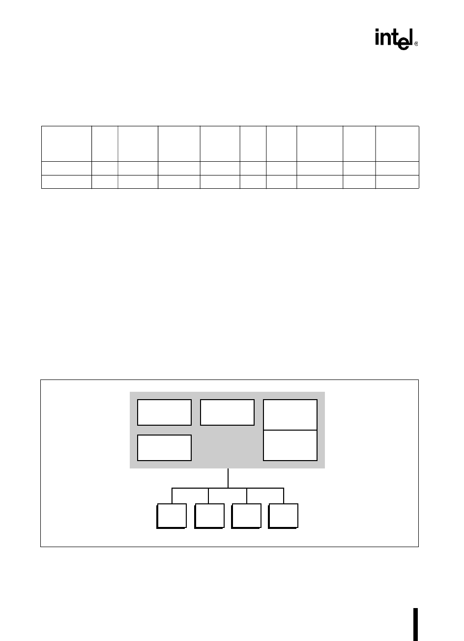
Figure 2-1 shows the major blocks within the device. The core of the device (Figure 2-2) consists
of the central processing unit (CPU) and memory controller. The CPU contains the register file
and the register arithmetic-logic unit (RALU). The CPU connects to both the memory controller
and an interrupt controller via a 16-bit internal bus. An extension of this bus connects the CPU to
the internal peripheral modules. In addition, an 8-bit internal bus transfers instruction bytes from
the memory controller to the instruction register in the RALU.
Figure 2-1. 8XC196NP and 80C196NU Block Diagram
Table 2-1. Features of the 8XC196NP and 80C196NU
Device Pins
ROM
(Note 1)
Register
RAM
(Note 2)
I/O Pins
(Note 3)
EPA
Pins
SIO
Ports
PWM
Channels
Chip-
select
Pins
External
Interrupt
Pins
8XC196NP 100 4 K 1024 64 4 1 3 6 4
80C196NU 100 0 1024 64 4 1 3 6 4
NOTES:
1. Nonvolatile memory is optional for the 8XC196NP, but is not available for the 80C196NU. The second
character of the device name indicates the presence and type of nonvolatile memory. 80C196NP =
none; 83C196NP = ROM.
2. Register RAM amounts include the 24 bytes allocated to core special-function registers (SFRs) and
the stack pointer.
3. I/O pins include address, data, and bus control pins and 32 I/O port pins.
A2801-01
Optional
ROM
Core
Clock and
Power Mgmt.
PTS
PWM
SIO
I/O
EPA
Interrupt
Controller


