8XC196NP, 80C196NU USER’S MANUAL
13-6
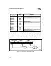
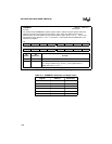
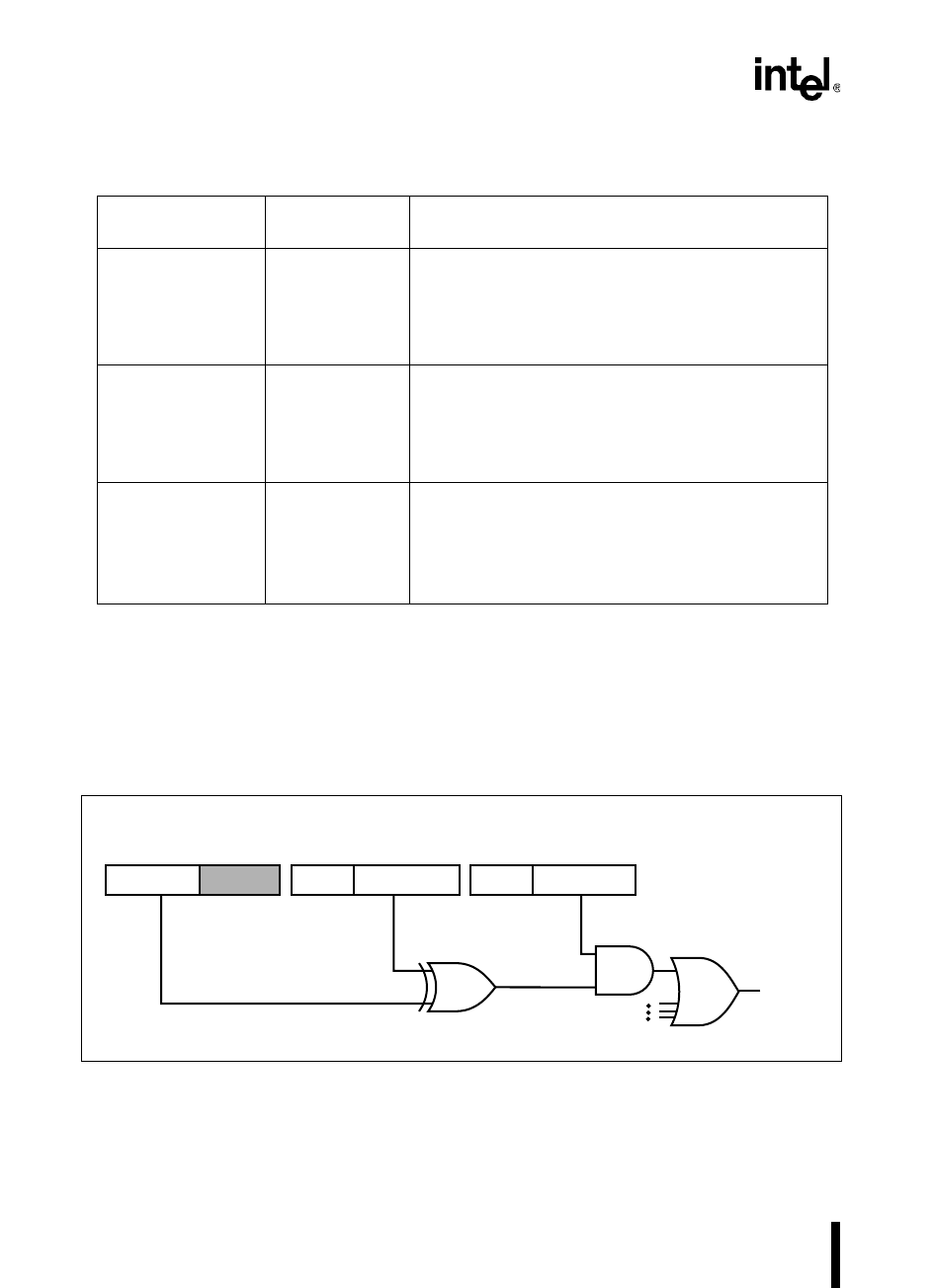
Figure 13-1 illustrates the device’s calculation of a chip-select output CSx# for a given external
memory address. The 12 most-significant bits of the external address are compared (XORed) bit-
wise with the 12 least-significant bits (BASE19:8) of the ADDRCOMx register. If all of the bits
match, CSx# is asserted. Additionally, if some bits do not match, CSx# is still asserted if, for each
non-matching bit in ADDRCOMx, the corresponding bit in ADDRMSKx is cleared. The 12 least-
significant bits are named MASK19:8 for their function in masking bits BASE19:8.
Figure 13-1. Calculation of a Chip-select Output
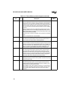
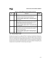
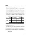
Table 13-3. Chip-select Registers
Register
Mnemonic
Address Description
ADDRCOM0
ADDRCOM1
ADDRCOM2
ADDRCOM3
ADDRCOM4
ADDRCOM5
1F40H
1F48H
1F50H
1F58H
1F60H
1F68H
Address Compare Register
This 16-bit register holds the upper 12 bits of the base
address of the address range assigned to CS
x
#.
ADDRMSK0
ADDRMSK1
ADDRMSK2
ADDRMSK3
ADDRMSK4
ADDRMSK5
1F42H
1F4AH
1F52H
1F5AH
1F62H
1F6AH
Address Mask Register
This register determines the size of the address range
(256 bytes–1 Mbyte).
BUSCON0
BUSCON1
BUSCON2
BUSCON3
BUSCON4
BUSCON5
1F44H
1F4CH
1F54H
1F5CH
1F64H
1F6CH
Bus Control Register
This register determines the bus configuration for external
accesses to the address range assigned to CS
x
#. The
bus parameters are 8- or 16-bit bus width, multiplexed or
demultiplexed address/data lines, and the number of wait
states inserted into each bus cycle.
A2386-02
0
7819 0111215 0111215
R • • • R
External Address ADDRCOM
x
ADDRMSK
x
bit
x
R • • • R
bit
x
bit
x
CS
x
#
BASE19:0 MASK19:0


