8XC196NP, 80C196NU USER’S MANUAL
13-12
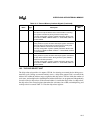
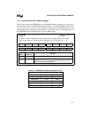
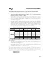
Use the following sequence to initialize the chip-select registers after reset:
1. Initialize chip-select output 0:
1.1. Clear ADDRMSK0.
1.2. Write to ADDRCOM0 to establish the desired base address.
1.3. Write to ADDRMSK0 to establish the desired address range.
1.4. Write the desired bus-parameter values to BUSCON0.
2. While executing in the address range defined in step 1 for chip-select output 0, use the
following sequence to initialize chip-select outputs 1–5. Begin with x = 1.
2.1. Load ADDRMSKx with 0FFFH.
2.2. Write to ADDRCOMx to establish the desired base address.
2.3. Write to ADDRMSKx to establish the desired address range.
2.4. Write the desired bus-parameter values to BUSCONx.
2.5. Repeat steps 2.1–2.4 for x = 2–5.
13.3.5 Example of a Chip-select Setup
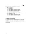
This section shows an example of setting up the chip-select unit and provides details of the chip-
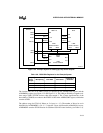
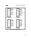
select output calculation. This example shows how to set up the chip-select registers for the sys-
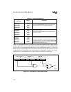
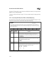
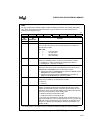
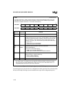
tem shown in Figure 13-5. For each address range, the BUSCONx register (see Figure 13-4) spec-
ifies the address/data multiplexing (bit 7), the bus width (bit 6), and the number of wait states (bits
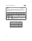
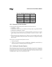
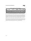
1, 0). Table 13-8 lists the characteristics of the three chip-select outputs and the corresponding
contents of BUSCONx.


