8XC196NP, 80C196NU USER’S MANUAL
11-8
11.6 RESETTING THE DEVICE
Reset forces the device into a known state. As soon as RESET# is asserted, the I/O pins, the con-
trol pins, and the registers are driven to their reset states. (Table B-5 on page B-13 lists the reset
states of the pins. See Table C-2 on page C-2 for the reset values of the SFRs.) The device re-
mains in its reset state until RESET# is deasserted. When RESET# is deasserted, the bus control-
ler fetches the chip configuration bytes (CCBs), loads them into the chip configuration registers
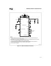
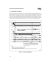
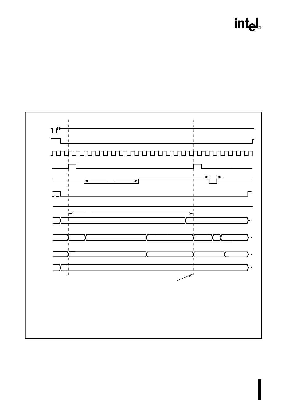
(CCRs), and then fetches the first instruction. Figure 11-7 shows the reset-sequence timing.
Figure 11-7. Reset Timing Sequence
RESET#
Pin
CLKOUT
ALE
RD#
A15:0
A19:16
00H
00H
18H CCB0
201AH
1AH
20H Strongly Driven
0FH Strongly Driven
20H Strong. Drv.
Notes:
1. Depends on number of wait states defined in CCB0.
2. If bus is multiplexed, AD15:8 strongly drive 20H.
2. If bus is demultiplexed, AD15:8 drive the data that is currently on the high byte of the internal bus.
CCB1
t
Note 1
Bus parameters defined by CCB0 (bus width, multiplexed
or demultiplexed mode, number of wait states) take effect
here (at start of second bus cycle). BUSCON0 is changed
here by value of CCB0.
2018H
A2417-02
Note 2
Internal
Reset
AD7:0
AD15:8
CS0#
NP
NU
t
CS5:1#


