5-31
MEMORY PARTITIONS
5.6.3 Example 3: Using 1-Mbyte Mode
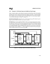
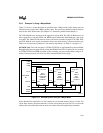
Figure 5-11 shows a system designed for operation in the 1-Mbyte mode. In this mode, code can
execute from any page in the 1-Mbyte memory space. The system uses both 8-bit and 16-bit buses
and uses the write-strobe mode. (See Chapter 13, “Interfacing with External Memory.”)
The 32K×8 RAM stores near data in the upper half of page 00H. The 32K×16 RAM stores far
data in page 01H. Using the WRL# and WRH# signals makes this RAM both byte- and word-
accessible. The 128K×16 flash memory stores code and far constants in pages FCH, FDH, FEH,
and FFH. With the write-signals connected as shown, the flash memory is word-accessible only.
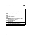
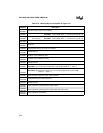
Table 5-14 lists the memory addresses. (For memory map details, see Table 5-3 on page 5-6.)
83C196NP only. The code and data in FF2000–FF2FFFH are implemented by internal ROM.
Remapping this area into page 00H by setting the REMAP bit (CCB1.2) makes the far constants
in FF2000–FF2FFFH of ROM accessible as near constants. An access to this address range is di-
rected to external memory if EA# is low and to internal ROM if EA# is high.
Figure 5-11. Example System Using the 1-Mbyte Mode
Notice that the microcontroller’s A1 line connects to a word-wide memory device’s A0 line. For
a byte-wide memory, the microcontroller’s A0 line selects the byte to be read. For a word-wide
memory, the microcontroller reads an entire word, then selects the required byte internally.
A2476-03
Flash
128Kx16
Code & Data
FC0000
FFFFFFH
CE#
Pages FC–FFH
A16:0
D15:0
OE# WE#
RAM
32Kx8
Data
008000–
00FFFFH
CE#
Page 00H
A14:0
D7:0
OE# WE#
8XC196NP,
NU
A17:0
AD15:0
RD#
WRH#
CS1#
CS0#
A14:0
AD7:0
A17:1
AD15:0
RAM
32Kx16
Data
010000–
01FFFFH
CE#
Page 01H
A14:0
D15:0
OE# WRH#
A15:1
AD15:0
CS2#
WRL#
WRL#


