11-7
MINIMUM HARDWARE CONSIDERATIONS
11.5 USING AN EXTERNAL CLOCK SOURCE
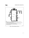
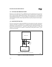
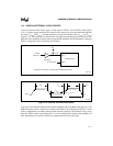
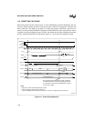
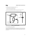
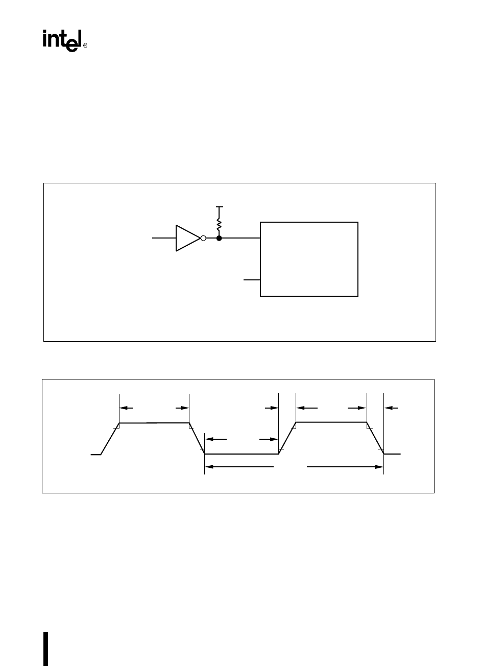
To use an external clock source, apply a clock signal to XTAL1 and let XTAL2 float (Figure
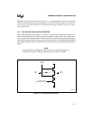
11-5). To ensure proper operation, the external clock source must meet the minimum high and
low times (T
XHXX
and T
XLXX
) and the maximum rise and fall transition times (T
XLXH
and T
XHXL
)
(Figure 11-6). The longer the rise and fall times, the higher the probability that external noise will
affect the clock generator circuitry and cause unreliable operation. See the datasheet for required
XTAL1 voltage drive levels and actual specifications.
Figure 11-5. External Clock Connections
Figure 11-6. External Clock Drive Waveforms
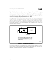
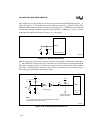
At power-on, the interaction between the internal amplifier and its feedback capacitance (i.e., the
Miller effect) may cause a load of up to 100 pF at the XTAL1 pin if the signal at XTAL1 is weak
(such as might be the case during start-up of the external oscillator). This situation will go away
when the XTAL1 input signal meets the V
IL
and V
IH
specifications (listed in the datasheet). If
these specifications are met, the XTAL1 pin capacitance will not exceed 20 pF.
4.7 kΩ
†
8XC196 Device
XTAL2
XTAL1
External
Clock Input
Clock Driver
No Connection
V
CC
A0274-02
†
Required if TTL driver is used. Not needed if CMOS driver is used.
4.7 kΩ
†
8XC196 Device
XTAL2
XTAL1
External
Clock Input
Clock Driver
No Connection
V
CC
A0274-02
†
Required if TTL driver is used. Not needed if CMOS driver is used.
A2119-02
T
XHXX
T
XLXX
T
XHXL
T
XLXL
0.3 V
CC
– 0.5 V
0.7 V
CC
+ 0.5 V
T
XLXH
0.7 V
CC
+ 0.5 V
0.3 V
CC
– 0.5 V
XTAL1


