9-7
PULSE-WIDTH MODULATOR
9.5 PROGRAMMING THE DUTY CYCLE
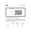
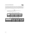
The value written to the PWMx_CONTROL register controls the width of the high pulse, effec-
tively controlling the duty cycle. The 8-bit value written to the control register is loaded into a
buffer, and this value is used during the next period. Use the following formula to calculate a de-
sired pulsewidth by extrapolating an appropriate value for PWMx_CONTROL from the range
00–FFH, and then write the value to the PWMx_CONTROL register.
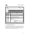
CON_REG0
Address:
Reset State:
1FB6H
FEH
The control (CON_REG0) register controls the clock prescaler for the three pulse-width modulators
(PWM0–PWM2).
7 0
8XC196NP
— — — — — ——CLK0
†
7 0
80C196NU
— — — — — — CLK1 CLK0
Bit
Number
Bit
Mnemonic
Function
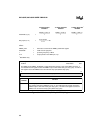
7:1 (NP)
7:2 (NU)
— Reserved; for compatibility with future devices, write zeros to these bits.
0 (NP) CLK0 Enable PWM Clock Prescaler
This bit controls the PWM output period by enabling or disabling the clock
prescaler (divide-by-two) on the three pulse width modulators (PWM2:0).
0 = disable; PWM output period is 512 state times
1 = enable; PWM output period is 1024 state times
1:0 (NU) CLK1:0 Enable PWM Clock Prescaler
These bits control the PWM output period on the three pulse-width
modulators (PWM2:0).
CLK1 CLK0
0 0 disable clock prescaler
0 1 enable divide-by-two prescaler; PWM output period is
1024 state times
1 X enable divide-by-four prescaler; PWM output period is
2048 state times
†
This bit was called SLOW_PWM in earlier documentation for the 8XC196NP.
Figure 9-4. Control (CON_REG0) Register


