B-7
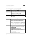
SIGNAL DESCRIPTIONS
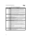
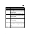
ALE O Address Latch Enable
This active-high output signal is asserted only during external memory cycles.
ALE signals the start of an external bus cycle and indicates that valid address
information is available on the system address/data bus (A19:16 and AD15:0
for a multiplexed bus; A19:0 for a demultiplexed bus). ALE differs from ADV# in
that it does not remain active during the entire bus cycle.
An external latch can use this signal to demultiplex address bits 0–15 from the
address/data bus in multiplexed mode.
BHE# O Byte High Enable
†
During 16-bit bus cycles, this active-low output signal is asserted for word reads
and writes and high-byte reads and writes to external memory. BHE# indicates
that valid data is being transferred over the upper half of the system data bus.
Use BHE#, in conjunction with A0, to determine which memory byte is being
transferred over the system bus:
BHE# A0 Byte(s) Accessed
0 0 both bytes
0 1 high byte only
1 0 low byte only
BHE# is multiplexed with WRH#.
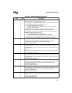
†
The chip configuration register 0 (CCR0) determines whether this pin
functions as BHE# or WRH#. CCR0.2 = 1 selects BHE#; CCR0.2 = 0 selects
WRH#.
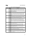
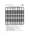
BREQ# O Bus Request
This active-low output signal is asserted during a hold cycle when the bus
controller has a pending external memory cycle.
The device can assert BREQ# at the same time as or after it asserts HLDA#.
Once it is asserted, BREQ# remains asserted until HOLD# is removed.
You must enable the bus-hold protocol before using this signal (see “Enabling
the Bus-hold Protocol” on page 13-32).
BREQ# is multiplexed with P2.3.
CLKOUT O Clock Output
Output of the internal clock generator. The CLKOUT frequency is ½ the internal
operating frequency (f). CLKOUT has a 50% duty cycle.
CLKOUT is multiplexed with P2.7.
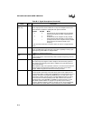
CS5:0# O Chip-select Lines 0–5
The active-low output CS
x
# is asserted during an external memory cycle when
the address to be accessed is in the range programmed for chip select
x
. If the
external memory address is outside the range assigned to the six chip selects,
no chip-select output is asserted and the bus configuration defaults to the CS5#
values.
Immediately following reset, CS0# is automatically assigned to the range
FF2000–FF20FFH (F2000–F20FFH if external).
CS5:0# is multiplexed with P3.5:0
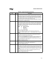
Table B-3. Signal Descriptions (Continued)
Name Type Description


