8XC196NP, 80C196NU USER’S MANUAL
13-22
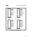
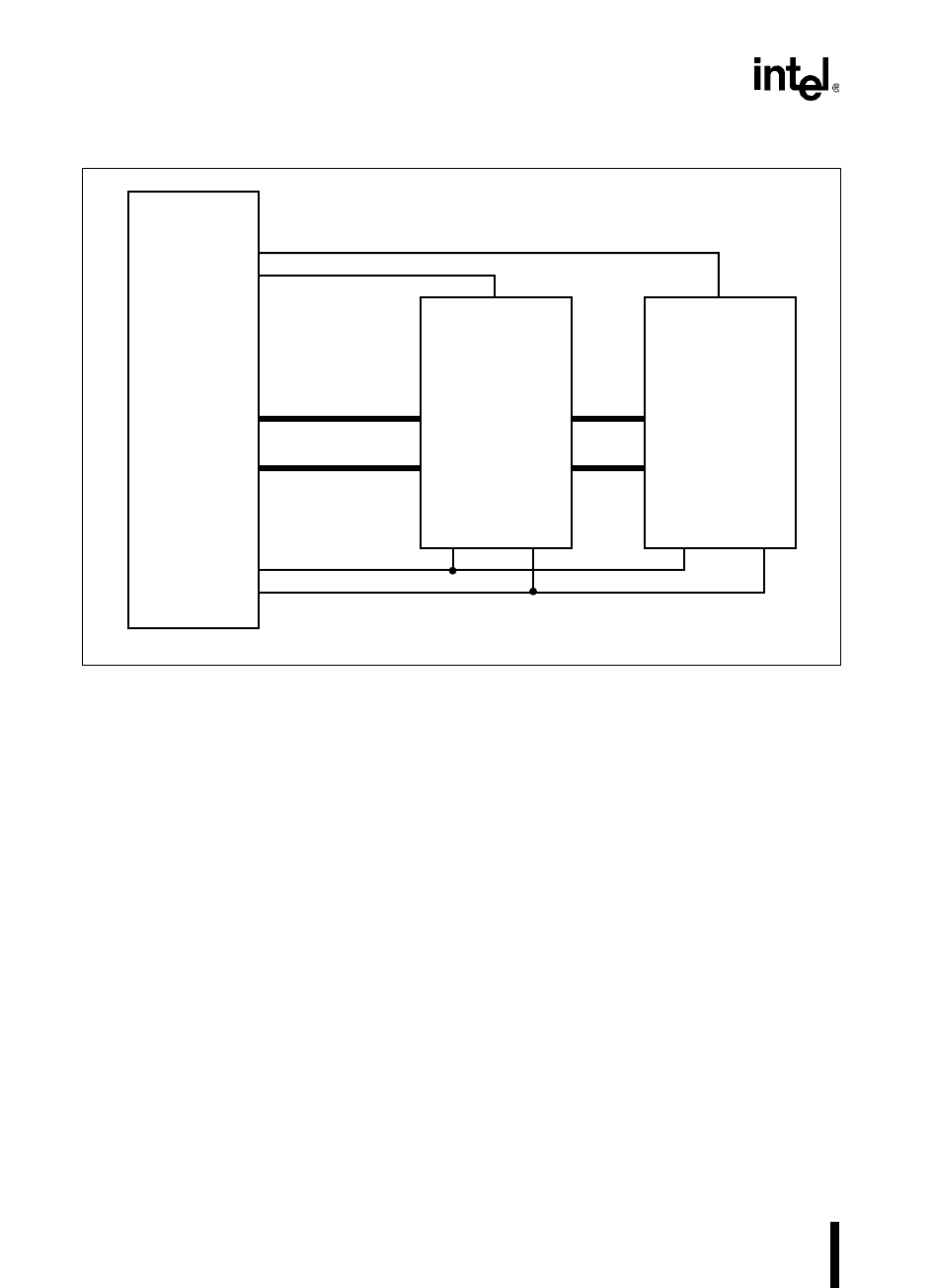
Figure 13-10. 16-bit External Devices in Demultiplexed Mode
13.5.2 16-bit Bus Timings
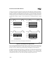
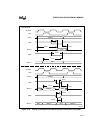
Figure 13-11 shows idealized 16-bit external-bus timings for the 8XC196NP. The signals are di-
vided into two groups: signals for a demultiplexed bus (top) and signals for a multiplexed bus
(bottom). Several bus signals are omitted from the figure to focus on a comparison of multiplexed
and demultiplexed buses. The timing parameters are addressed in “Comparison of Multiplexed
and Demultiplexed Buses” on page 13-26. Comprehensive timing specifications for both the
8XC196NP and the 80C196NU are shown in Figures 13-20 through 13-23.
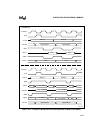
CLKOUT and ALE are the same in multiplexed and demultiplexed buses. The CLKOUT period
is twice the internal oscillator period (2t). The bus cycles shown here, which have no wait states,
require two CLKOUT periods (two state times).
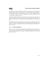
The rising edge of the address latch enable (ALE) indicates that the device is driving an address
onto the bus (A19:16 and AD15:0). The device presents a valid address before ALE falls. In a
multiplexed system, the ALE signal is used to strobe a transparent latch (such as a 74AC373),
which captures the address from AD15:0 and holds it while the bus controller puts data onto
AD15:0.
CS1#
CS0#
A19:0
AD15:0
RD#
WR#
8XC196
Flash
256K×16
CS#
A17:0
D15:0
A17:0
D15:0
CS#
WE#OE# WE#OE#
A18:1
AD15:0
A18:1
AD15:0
A2438-03
Flash
256K×16


