B-13
SIGNAL DESCRIPTIONS
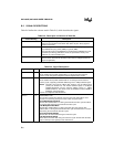
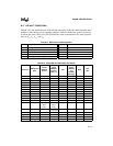
B.3 DEFAULT CONDITIONS
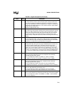
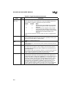
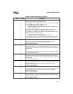
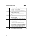
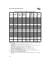
Table B-5 lists the default functions of the I/O and control pins of the 8XC196NP and 80C196NU
with their values during various operating conditions. Table B-4 defines the symbols used to rep-
resent the pin status. Refer to the DC Characteristics table in the datasheet for actual specifica-
tions for V
OL
, V
IL
, V
OH
, and V
IH
.
Table B-4. Definition of Status Symbols
Symbol Definition Symbol Definition
0 Voltage less than or equal to V
OL
, V
IL
MD0 Medium pull-down
1 Voltage greater than or equal to V
OH
, V
IH
MD1 Medium pull-up
HiZ High impedance WK0 Weak pull-down
LoZ0 Low impedance; strongly driven low WK1 Weak pull-up
LoZ1 Low impedance; strongly driven high ODIO Open-drain I/O
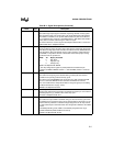
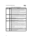
Table B-5. 8XC196NP and 80C196NU Pin Status
Port Pins
Multiplexed
With
During
RESET#
Active
Upon
RESET#
Inactive
(Note 11)
Idle
Power-
down
(NP/NU)
and
Standby
(NU only)
Hold
Bus
Idle
P1.3:0 EPA3:0 WK1 WK1 (Note 1) (Note 1) (Note 1) —
P1.4 T1CLK WK1 WK1 (Note 1) (Note 1) (Note 1) —
P1.5 T1DIR WK1 WK1 (Note 1) (Note 1) (Note 1) —
P1.6 T2CLK WK1 WK1 (Note 1) (Note 1) (Note 1) —
P1.7 T2DIR WK1 WK1 (Note 1) (Note 1) (Note 1) —
P2.0 TXD WK1 WK1 (Note 1) (Note 1) (Note 1) —
P2.1 RXD WK1 WK1 (Note 1) (Note 1) (Note 1) —
P2.2 EXTINT0 WK1 WK1 (Note 1) (Note 1) (Note 1) —
P2.3 BREQ# WK1 WK1 (Note 1) (Note 1) (Note 1) —
P2.4 EXTINT1 WK1 WK1 (Note 1) (Note 1) (Note 1) —
P2.5 HOLD# WK1 WK1 (Note 1) (Note 1) Force 0 —
P2.6 HLDA# WK1 WK1 (Note 1) (Note 1) 0 —
P2.7 CLKOUT CLKOUT
active;
LoZ0/1
CLKOUT
active;
LoZ0/1
(Note 1) (Note 2) (Note 1) —
P3.0 CS0# WK1 1 (NP only)
0 (NU only)
(Note 3) (Note 3) (Note 4) —
P3.5:1 CS5:1# WK1 WK1 (Note 3) (Note 3) (Note 4) —
P3.6 EXTINT2 WK1 WK1 (Note 1) (Note 1) (Note 1) —
P3.7 EXTINT3 WK1 WK1 (Note 1) (Note 1) (Note 1) —
P4.2:0 PWM2:0 WK1 WK1 (Note 1) (Note 1) (Note 1) —


