MT90840 Preliminary Information
2-234
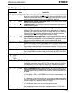
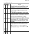
22 66 F0i/o Serial Port Frame Synchronization (Bidirectional). This 8 kHz frame pulse
signal indicates the TDM 125 µsec frame boundary on the serial data port. This
pin is compatible with both ST-BUS/MVIP and GCI formatted framing signals.
In TM1 this pin is an input, and the MT90840 senses the polarity of this frame
pulse and automatically adapts the serial data port timing to the applicable format
(ST-BUS or GCI).
In TM2 with SFDI =1 this signal is an input, and its expected format is determined
by the SPFP bit in the GPM Register.
In TM2 (with SFDI =0), and in TM3, this signal is an output, generated from the
internal timing and synchronized to the SPCKo output clock. The polarity of the F0
pulse is determined by the SPFP bit in the GPM Register.
In TM4 this pin is not used.
23 67 C4/8R2 C4/8R2 Serial Clock Reference Input 2. When enabled by the C4/8R bit (low) in
the TIM Register, this input receives the 4.096 or 8.192 MHz serial port clock
reference. If the C4/8R bit is set high, or if the INTCLK bit is set high, this input is
ignored by the MT90840. (See pin description for C4/8R1.)
28-31 70-73 CTo3-
CTo0
External Control Lines 3 to 0 (Output). Output signals generated from the
MT90840 Transmit Path Connection Memory (TPCM). The four serial CTo output
lines represent the contents of the four CT bits in the TPCM, and are clocked at the
parallel port rate (up to 19.44 MHz). See Per-Channel Functions section.
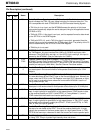
34-41 81-88 PDo7-PDo
0
Parallel Data Output Port 7 to 0 (Output). These eight outputs carry the parallel
port data bytes in the transmit direction and operate at data rates up to 19.44
Mbyte/s.
42 89 PPFTi/o Parallel Port Framing, Transmit (Bidirectional). This signal delineates the start
of a new data frame at the PDo0-7 lines on the transmit parallel port. Normally an
output, when the PFDI bit in the TIM Register is set high PPFT becomes an input,
and is used to receive the frame reference from another MT90840. Used in all
timing modes except TM3.
45-52 92-99 PDi7-0 Parallel Data Input Port 7 to 0 (Input). These eight inputs carry the parallel port
data bytes in the receive direction and operate at data rates up to 19.44 Mbyte/s.
55 6 PCKR Parallel Port Clock, Receive (Input). This is a 19.44, 16.384, or 6.48 MHz clock
input. It might typically be provided by a high speed framer. PCKR clocks in data
on the receive parallel port (PDi7-0 and PPFRi). In Timing Modes 2, 3, and 4,
PCKR clocks both the transmit and receive parallel ports.
56 7 PCKT Parallel Port Clock, Transmit (Input). This is a 19.44, 16.384, or 6.48 MHz clock
input. It might typically be provided by a high speed framer. In TM1 PCKT clocks
out the data on the transmit parallel port (PDo0-7, CTo0-3, and PPFTo). In TM2,
TM3, & TM4, this input is ignored.
57 8 PPFRi Parallel Port Framing, Receive (Input). This 8 kHz frame pulse input determines
the start of a new frame at the PDi0-7 lines of the receive parallel port. It might
typically be connected to the frame pulse output of a high speed framer. In TM3,
PPFRi is the frame sync reference for both the transmit and receive parallel ports.
58 9 TDI Test Data (Input). JTAG serial test instructions and data are shifted in on this pin
on rising TCK. This pin is pulled high internally when not driven.
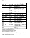
Pin Description (continued)
Pin #
Name Description
84 100


