


MT90840 Preliminary Information
2-264
‡ Typical figures are at 25°C and are for design aid only: not guaranteed and not subject to production testing.
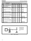
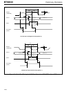
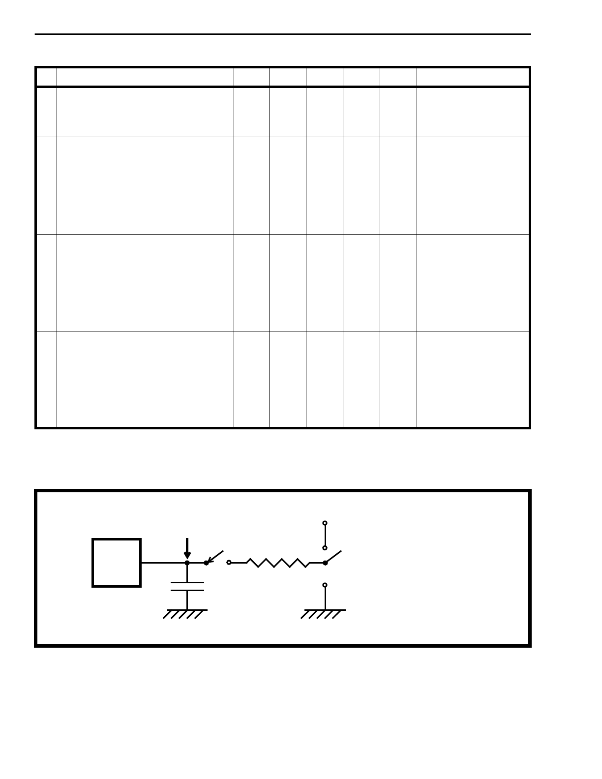
Figure 17 - Output Test Load
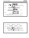
10 STo Delay from High-Z to Active
2.048 and 4.096 Mbps (TM2 &TM3)
2.048 and 4.096 Mbps (TM1)
8.192 Mbps (STio0-3)
t
za
38
50
26
ns
ns
ns
C
L
=30pF, R
L
=1K
11 STo Output Delay from SPCKo
(TM2 & TM3, 2.048 and 4.096 Mbps)
STo Output Delay from 4.096 MHz C4/8
input (TM1)
STo 8.192 Mbps Output Delay from
C4/8 input (TM1, 2 & 3; STi/o0-3)
t
sod
40
64
52
72
28
43
ns
ns
ns
ns
ns
ns
C
L
=30pF
C
L
=150pF
C
L
=30pF
C
L
=150pF
C
L
=30pF
C
L
=150pF
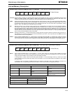
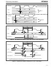
12 STi Input Setup Time from SPCKo
output edge (2.048 and 4.096 Mbps)
STi Input Setup Time from C4/8 input
edge in TM1 (2.048 and 4.096 Mbps)
STi Input Setup Time from C4/8 input
edge at 8.192 Mbps (STi/o0-3)
t
stis
28
41
0
0
ns
ns
ns
SPCKo C
L
=30pF
SPCKo C
L
=150pF
TM1 and TM2,
STi0-3, STo0-3
13 STi Input Hold Time from SPCKo output
edge (2.048 and 4.096 Mbps)
STi Input Hold Time from C4/8 input
edge in TM1 (2.048 and 4.096 Mbps)
STi Input Hold Time from C4/8 input
edge at 8.192 Mbps
t
stih
9
2
20
13
ns
ns
ns
SPCKo C
L
=30pF
SPCKo C
L
=150pF
TM1 and TM2,
STi0-3, STo0-3
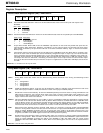
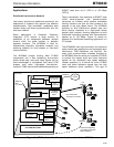
AC Electrical Characteristics - Voltages are with respect to ground (V
SS
) unless otherwise stated.
Characteristics Sym Min Typ
‡
Max Units Test Conditions
Output
Pin
Test Point
C
L
V
SS
S1
R
L
V
DD
S2
V
SS
S1 is open circuit except
when testing output levels
or high impedance states.
S2 is switched to VDD or
V
SS
when testing output
levels or high impedance
states.