


MT90840 Preliminary Information
2-262
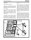
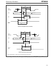
synchronization scheme may be used in applications
such as the proposed MVIP multi-chassis level 3
interface (MC-3 system) utilizing point-to-point or
point-to-multipoint switching connections.
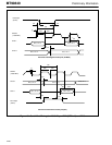
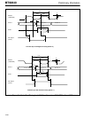
When the MT90840 operates in a ring application,
the Parallel Data Bypass mode is provided to allow
all or part of the received input parallel data to be
bypassed to the output parallel port feeding the ring
back with the data which is not destined for the local
station. The data destined for the local station can be
dropped through CPU programming. In this mode,
the CPU has full control of the outgoing bandwidth
(from the serial interface to the high speed link) so
that it does not contend with the bypassed data.
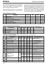
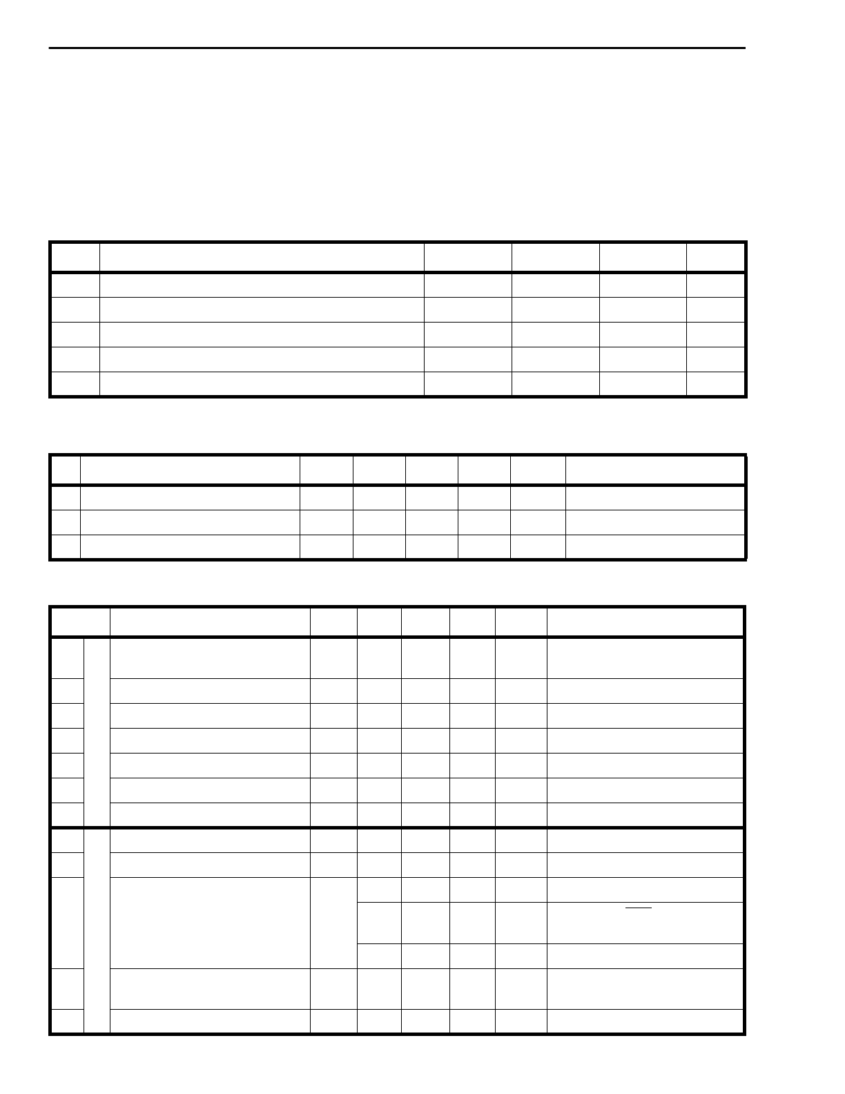
* Exceeding these values may cause permanent damage. Functional operation under these conditions is not implied.
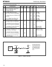
‡ Typical figures are at 25°C and are for design aid only: not guaranteed and not subject to production testing.
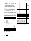
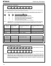
Absolute Maximum Ratings*
Parameter Symbol Min Max Units
1 Supply Voltage V
DD
06V
2 Voltage on any I/O pin V
I
V
SS
-0.3 V
DD
+0.3 V
3 Continuous Current at Digital Outputs I
O
40 mA
4 Storage Temperature T
S
-65 +150 °C
5 Package Power Dissipation P
D
2W
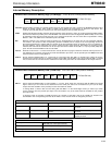
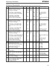
Recommended Operating Conditions - Voltages are with respect to ground (V
SS
) unless otherwise stated.
Characteristics Sym Min Typ Max Units Test Conditions
1 Operating Temperature T
OP
-40 +85 °C
2 Positive Supply V
DD
4.75 5.0 5.25 V
3 Input Voltage V
I
0V
DD
V
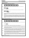
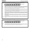
DC Electrical Characteristics - Voltages are with respect to ground (V
SS
) unless otherwise stated.
Characteristics Sym Min Typ
‡
Max Units Test Conditions/Pins
1
I
N
P
U
T
S
Supply Current at
19.44 Mbyte/sec & 4 Mbps
I
DD
100 160 mA Outputs unloaded
2 Input High Voltage V
IH
2.0 V TTL inputs (most pins)
3 Input Low Voltage V
IL
0.8 V TTL inputs (most pins)
4 Input High-Going Threshold V
T+
2.8 4.2 V Schmitt inputs
5 Input Low-Going Threshold V
T-
0.9 1.8 V Schmitt inputs
6 Input Leakage (I/O pins) I
IL
50 µAV
I
between V
SS
and V
DD
7 Input Pin Capacitance C
I
10 pF
8
O
U
T
P
U
T
S
Output High Voltage V
OH
2.4 V Sourcing I
OH
9 Output Low Voltage V
OL
0.4 V Sinking I
OL
10 Output High Current
(sourcing at V
OH
)
or
Output Low Current
(sinking at V
OL
)
I
OH
or
I
OL
9 mA Pins: STi4-7, STo4-7
16 mA TDO, RPA, DTA, AD7-0, F0,
SPCKo, STi0-3, STo0-3
28 mA PDo0-7, CTo3-0, PPFTo
11 High Impedance Leakage I
OZ
5 µAV
O
between V
SS
and V
DD.
Pins: PDo0-7, CTo3-0
12 Output Pin Capacitance C
O
10 pF