


MT90840 Preliminary Information
2-254
I/O pin of the IC. The operation of the boundary-scan
circuitry is controlled by a Test Access Port (TAP)
Controller.
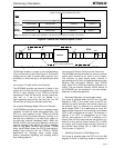
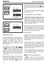
Test Access Port (TAP)
The Test Access Port (TAP) has five signals and
provides access to the test logic defined by the JTAG
standard.
The TAP has the following connections:
• Test Clock Input (TCK)
TCK provides the clock for the test logic. TCK is
independent of the MT90840 functional clocks;
this permits serial shifting of test data along the
Boundary-Scan chain concurrent with the
normal operation of the MT90840.
• Test Mode Select Input (TMS)
The signal at TMS selects the operational mode
of the TAP Controller. The TMS signals are
sampled on the rising edge of TCK. This pin is
pulled high internally when not driven.
• The Test Data Input (TDI)
Serial instructions and test-data are shifted in
at this pin. Serial information is passed to the
instruction register, the boundary scan (test)
register, or the bypass register, depending on
the present mode of the TAP controller. TDI is
sampled on the rising edge of TCK. This pin is
pulled high internally when not driven.
• The Test Data Output (TDO)
Serial data is shifted out on this pin. Depending
on the present mode of the TAP controller, data
will come from one of: the instruction register,
the boundary scan register or the bypass
register. TDO is clocked out on the falling edge
of TCK. When no data is being shifted, the TDO
driver is set to a high-impedance state.
• TRST:(Test reset input)
Asynchronously initializes the TAP controller by
putting it in the
Test-Logic-Reset
state. This pin
is pulled high internally when not driven.
One additional pin influences the boundary scan test
operation:
• IC: (Manufacturing test pin)
This pin is an IEEE 1149 compliance-enable
pin, and must be connected to Vss for proper
boundary scan operation (and normal chip
operation).
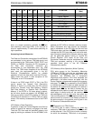
Boundary-Scan Instruction Register
In accordance with the IEEE 1149.1 standard, the
MT90840 uses public instructions listed in Table 3 -
“Instruction Register”. The MT90840 JTAG Interface
contains a two bit instruction register. Instructions
are serially loaded into the Instruction Register from
the TDI pin when the TAP Controller is in its Shift-IR
state. Subsequently, the instructions are decoded to
achieve two basic functions: to select the test data
register that may operate while the instruction is
current and to define the serial test data register path
that is used to shift data between TDI and TDO
during data register scanning.
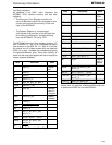
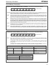
I[0:1] Instruction Description
[00] EXTEST Boundary-Scan
Register selected,
Test enabled
This instruction is specifically provided to allow board-level interconnect
testing of opens, bridging errors etc.
When the EXTEST instruction is executed, the MT90840 core logic is
isolated from the I/O pins, and the state of the I/O pins is determined by
the boundary-scan register. I/O data for this instruction is pre-loaded into
the boundary-scan register with the SAMPLE/PRELOAD instruction.
[01]
[10]
SAMPLE/
PRELOAD
Boundary-Scan
Register selected,
Test disabled
Two functions can be performed by the use of this instruction. It allows a
SAMPLE (‘snapshot’) of the normal operation of the MT90840 to be
taken for examination. And, prior to the selection of another test
operation, a PRELOAD can place data values into the latched parallel
outputs of the Boundary-Scan cells. During the execution of the
instruction, the on-chip logic operation is not hampered in any way.
[11] BYPASS Bypass Register
selected,
Test disabled
This instruction is used to BYPASS the MT90840 while performing
boundary-scan testing on other devices with scan registers in the same
serial register chain. The MT90840 is allowed to function normally. This
instruction is automatically loaded upon TRST, as specified in
IEEE1149.1
Table 3 - Boundary-Scan Instruction Register