MT90840 Preliminary Information
2-250
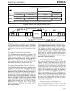
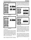
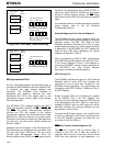
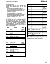
Figure 14a - 8.192 Mbps TPDM Addressing
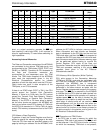
Figure 14b - 8.196 Mbps RPCM Addressing
Microprocessor Port
An 8-bit multiplexed parallel microprocessor port is
provided on the MT90840 to allow an attached CPU
to configure and read internal registers and
memories. The MT90840 CPU interface is
compatible with Motorola, National and Intel
Multiplexed Bus CPUs and adapts itself to the
appropriate bus-type control signal timing without
any mode selection.
The MT90840 CPU interface signals are AD0-7
(Data and Address), ALE/AS, DS/RD, R/W\WR, CS
and DTA. The parallel microprocessor interface
provides the CPU with access to the internal
configuration registers, and the Connection and Data
Memories for both the transmit and receive paths.
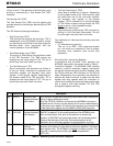
Connection memories are read/write, Data Memories
are read only, and the control register senses are
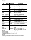
shown in Table 2.
Accesses from the microport to the Connection and
Data Memories are multiplexed with accesses from
the input and output TDM ports. This can cause
variable data acknowledge delays which are
communicated to the CPU by the DTA output signal.
Note that if the parallel port clocks PCKR & PCKT or
serial port clocks C4/8R1 & C4/8R2 are not present
during an internal memory access, the DTA output
signal may be held HIGH until the clocks are applied
again.
For complete details on the Microprocessor Interface
timing signals, refer to the AC Electrical
Characteristics section.
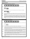
Address Mapping of the Internal Registers
The MT90840 provides internal registers which are
used by the CPU to configure the device in the various
operation modes. The IMS, TIM, GPM and ALS
Registers should be initialized by the CPU on every
system power-up before any internal memory access
is performed. In the MT90840, the AD7 address pin
must be kept LOW when addressing the internal
registers, as depicted in Table 2.
When input address pin AD7 is HIGH, input address
pins AD0-AD6 are used together with bits HA7-HA11
in the Control Register to form a 12-bit address to
access the MT90840 internal memory selected by
the SEL2-SEL0 bits. See Internal Memory
Description for memory address mapping.
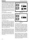
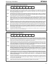
IRQ Interrupt Pin
The MT90840 provides the output pin IRQ (Interrupt
Request) which is active HIGH and indicates the
occurrence of one or more error conditions in the
MT90840 timing operations. The occurrences are
indicated by bits PPCE, RXPAA, TXPAA and FSA in
the ALS Register.
Except for cases where the indications are masked
by the MSK3-0 bits in the ALS Register, the
occurrence of any indication causes an IRQ interrupt
to be generated to the CPU. When an interrupt is
masked by MSK3-0 bits, the IRQ output will not be
activated. However, the interrupt indication will still
be provided in the ALS bits.
To cause the IRQ output signal or the indication bits
to return to LOW again, the CPU can write any value
to the ALS Register (normally the Mask bits are
re-written to clear the IRQ pin).
DTA Data Transfer Acknowledgment Pin
The DTA pin is driven LOW by internal logic, to
indicate to the CPU that a data bus transfer is
complete. When the bus cycle ends, this pin drives
HIGH and then switches to high-impedance. If a
.
.
STi0, Ch0
STi0, Ch1
000H
001H
TPCM Contents:
87
6
43
21
0
Stream
Channel
Bits 8:7 select one of 8 streams.
Bits 6:0 select one of 128
channels per stream.
STi3, Ch126
STi4, Ch127
1FEH
1FFH
5
Serial Input
Channel
TPDM
Address
CPU Port Addressing:
10 6 43
21
0
Stream
Channel
Address Bus
CAR
5
.
.
STo0, Ch0
STo0, Ch1
000H
001H
CPU Port Addressing:
10 6 43
21
0
Stream
Channel
Address Bus
CAR
STo3, Ch126
STo4, Ch127
1FEH
1FFH
5
RPCM
Address
Serial Output
Channel


