


Preliminary Information MT90840
2-241
streams, and trigger the PPCE interrupt bit. PPCE
will be triggered by PPFRi moving from the expected
time, but PPCE will not be triggered by a missing
PPFRi. If the PPFRi input is held asserted, the
parallel I/O will “lock up” and operation will be
disrupted (including CPU access to the TPCM).
The PPFTi framing in TM1 with PFDI=1 operates
similarly, using PCKT, but the PPCE interrupt does
not monitor PPFTi. Instead, the TXPAA bit indicates
that the PPFTi input is out of phase with F0i.
Output Driver Enable Control Capability
The MT90840 provides a bit (ODE) in the IMS
Register that places all data outputs of the device
(parallel and serial) in a high impedance state. The
ODE bit (Output Drive Enable) is automatically set
low by the reset input pulse applied to the device
during system power up. When low, the ODE bit
disables all TDM outputs of the MT90840 while
Connection Memory initialization is performed by the
CPU. This function is useful to avoid data collision
when the MT90840 is sharing a transmit parallel bus
with other devices. When ODE is set high, individual
parallel and serial port time slots are controlled by
the OE bits in TPCM High and RPCM High.
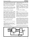
Timing and Switching Control
The MT90840 supports four major timing/switching
modes:
• TM1/Ring Master: PDo timing slaved to STi/o
timing, Receive Path has elastic buffer enabled;
• TM2/Ring Slave: STi/o timing slaved to PDi timing,
fixed delay in Receive Path;
• TM3/Bus Slave: PDo and PDi tied together, STi/o
timing slaved to parallel bus timing;
• TM4/Parallel Switching: 2430 (or 2048) channel
switching from PDi to PDo.
The TM1-0 bits in the TIM Register are used to
select the timing modes. The PFDI and SFDI bits in
the same register can be used to enable
parallel-device sub-modes of TM1 and TM2
respectively. In all MT90840 timing modes, the
throughput delay when performing time interchange
functions of grouped channel data is constant,
maintaining the frame integrity of the input and
output data.
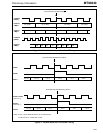
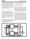
Timing Mode 1 (TM1) - Ring Master
Asynchronous Parallel Port With ST-BUS Clock
Master
Timing Mode 1 is used where the main TDM clock
reference resides on the serial port side of the
system. (An example is a node which is the clock
master on a ring network.) Timing on the transmit
parallel port is tightly tied to the serial port. The
receive parallel port timing is elastic; there is an
elastic buffer in the Receive Path and the Bypass
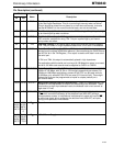
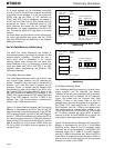
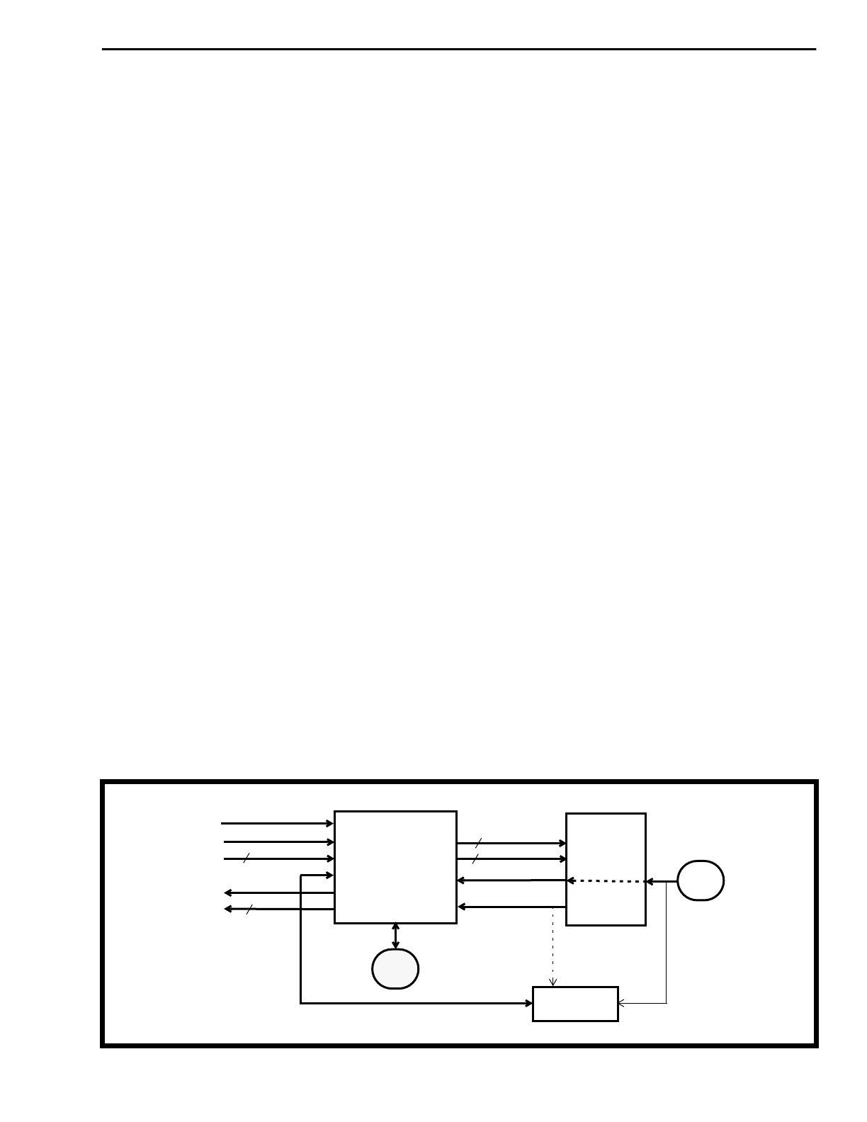
Path. See Figure 5a for a connection example.
In TM1, the MT90840 receives the serial port frame
pulse (F0i) and serial clock (C4/8R1 or C4/8R2). The
MT90840 then generates the parallel port output
frame pulse (PPFTo) synchronized to F0i. The
transmit parallel port is fixed in phase relative to the
serial port. (A fixed offset of 3.8 µsec exists between
F0i and PPFTo due to serial-to-parallel conversion.)
The transmit path does not provide an elastic buffer,
and therefore the parallel port TX clock (PCKT) must
be tightly locked (in frequency) to the serial port C4/8
and F0i clocks. (Jitter less than +/- 100nsec.)
The receive parallel port timing may be of any phase
relative to the serial and transmit-parallel ports in
Figure 5a - Timing Mode 1 Configuration
8
8
8 kHz RX
Data RX
TX Clock
8 kHz TX
Data TX
PCKR
PPFRi
PDi0-7
PCKT
PPFTo
PDo0-7
STi0-7
STo0-7
F0i
C4/8R1
8
STi/o 0-7
8
STi/o 0-7
4.096
MT90840
RX Clock
CPU
ST-BUS
Components
or 8.192 MHz
8 kHz
8 kHz
Source
PLL