


MT90840 Preliminary Information
2-256
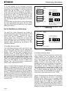
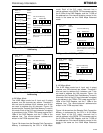
Register Description
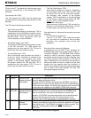
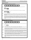
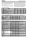
Interface Mode Selection Register (IMS) - READ/WRITE
76543210
DR1 DR0 PPS1 PPS0 ODE 0 0 FDC
DR1-0 Serial Port Data Rate Selection. Select one of three different data rates at the serial inputs and outputs of the
MT90840.
DR1 DR0 Data Rate
0 0 2.048 Mbps
0 1 4.096 Mbps
1 0 8.192 Mbps
1 1 reserved
PPS1-0 Parallel Port Data Rate Selection. Select one of three different data rates for the parallel port of the MT90840.
PPS1 PPS0 Data Rate
0 0 reserved. Do not use.
0 1 6.480 Mbyte/s.
1 0 19.44 Mbyte/s.
1 1 16.384 Mbyte/s.
ODE Output Drive Enable. When LOW, forces the MT90840 output-buffers on the serial and parallel data ports into the
high impedance state (STo0-STo7, STi0-STi7, and PDo0-7). If this output is HIGH, all channels have their output
drive enable controlled by the per-channel OE bits of Transmit Connection Memory High, or Receive Connection
Memory High.
FDC Full Direction Control. This bit should only be set HIGH at the 2.048 Mbps serial rate. When FDC is set HIGH, each
time slot on each of the 16 ST-BUS pins can be individually configured as input or output. Up to 512 serial channels
can be “inserted” onto the Transmit parallel port, or up to 512 parallel channels can be “dropped” to the serial port.
Individual channel direction is controlled by the DC bits in the RPCM High. When FDC is LOW, the number of input
and output time slots are “balanced”, and setting a nominal input to be an output causes the same-number output
time slot on the same-number STo pin to become an input. For applications at 4.096 and 8.192 Mbps, this bit should
be LOW.
Note: Bits 1 & 2 must be set to 0 by the CPU.
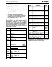
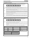
TM1-0 Timing Mode control bits. Define the four different timing modes described in the Timing and Switching Control
section.
0 0 Timing Mode 1
0 1 Timing Mode 2
1 0 Timing Mode 3
1 1 Timing Mode 4
C4/8R C4/8R Input Reference Select. If set high, this bit enables the 4.096 or 8.192 MHz serial port reference clock to be
taken from input pin C4/8R1. If LOW, the reference is taken from input pin C4/8R2 (default).
TCP Parallel Port Transmit Clock Polarity. To allow the MT90840 parallel port transmit clock to comply with different 155
Mbps framer backplanes, TCP controls which edge of the clock is used to transmit data at the parallel port. (The
clock is PCKT in TM1 or PCKR in TM2, 3, & 4). The TCP bit allows the rising (TCP=LOW) or the falling (TCP=HIGH)
edges of the transmit clock to be selected.
INTCLK Internal 4.096 MHz Clock Divider. For use in TM2, in 19.44 or 16.384 MHz parallel-port applications. This bit controls
the operation of the internal clock divider driven by PCKR. When INTCLK is set HIGH the internal 4.096 MHz clock
(and the SPCKo output) are generated by dividing down the PCKR clock. When INTCLK is set LOW, the C4/8R bit
controls the source for the serial clock reference. In TM3 and TM4 the MT90840 automatically sets itself in the
internal divider mode and the state of INTCLK has no effect. In TM1 this bit is must be set LOW.
SFDI Serial Frame Pulse Direction Control. Normally LOW, unless it is necessary to operate multiple parallel MT90840
devices in Timing Mode 2. When set HIGH, the F0 line becomes an input and this MT90840 is synchronized to the
timing of another MT90840 generating the F0o, and using the same 4.096 or 8.192 MHz reference input. One
MT90840 in TM2 with SFDI LOW can control several MT80940s with SFDI HIGH. When SFDI is set HIGH, INTCLK
is ignored, and SPFP in the GPM register must be set to the expected F0i polarity.
PFDI Parallel Frame Pulse Direction Control. Normally LOW, unless it is necessary to operate multiple parallel MT90840
devices in Timing Mode 1. When set HIGH, the PPFT pin becomes an input and this MT90840 is synchronized to the
timing of another MT90840 generating the PPFTo. One MT90840 in TM1 with PFDI LOW can control several
MT80940s with PFDI HIGH. When PFDI is HIGH, PPFP in the GPM register must be set to the expected PPFTi
polarity.
Note: Bit 7 must be set to 0 by the CPU.
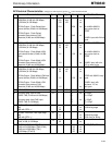
Timing Mode Register (TIM) - READ/WRITE
76543210
TM1 TM0 C4/8R TCP INTCLK
SFDI PFDI
0