


Preliminary Information MT90840
2-257
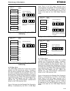
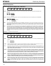
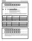
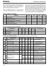
General Purpose Mode Register (GPM) - READ/WRITE
76543210
BPD6 BPD5 BPD4 PPFP SPFPBPD7 DIN BPE
BPD7-4 Block-Programming Data bits 7-4. These bits carry the value to be loaded into the TPCM-High or RPCM-High
memory when the Memory Block-Programming feature is activated. When BPE is set HIGH, the contents of bits
BPD7-4 are loaded into the four most significant bits of TPCM-High or RPCM-High, and the four least significant bits
of TPCM-High or RPCM-High are zeroed.
PPFP Parallel Port Frame pulse Polarity. Used to program the polarity of the PPFT frame pulse. If PPFP is set HIGH, the
frame boundaries at the Parallel Port output will occur when PPFT pulse signal is HIGH. If PPFP is set LOW, the
PPFT output will indicate frame boundaries with a LOW active pulse. The transmit edge for the generation of PPFT,
as well as PDo and CTo, is determined by TCP in the TIM Register.
DIN Device Initialization. This bit is used in TM1 and TM2 to center the phase relation between the parallel port clocks
and the serial port clock. It can be set HIGH by the CPU after the serial and parallel port rates are written in the IMS
Register, and the input clocks are stable. If the MT90840 internal divider is used (INTCLK bit = HIGH), or if TM4 or
TM3 is selected, this bit is not used. This bit is automatically returned low after 8 frames, and clears all interrupt
source bits in the ALS register as long as it is HIGH. The Connect Memories should not be programmed while DIN is
asserted.
SPFP Serial Port Framing Polarity. In TM2 and TM3 this bit defines the format of the serial port frame pulse F0o, and the
clock SPCKo. If SPFP is HIGH, F0o is set as a positive pulse with GCI timing. If SPFP is LOW, F0o is set as a
negative pulse with ST-BUS timing. In TM2 with SFDI set HIGH, this bit specifies the expected F0i input polarity. In
TM1, the F0i input polarity is automatically detected, and this bit is ignored. See the interface timing specifications.
BPE Block-Programming Enable. This bit activates the memory block-programming feature. It can be set high after the
SEL0-2 bits in the Control Register are set to select the memory to be programmed. The BPE and BPD7-4 bits in this
register must be defined in the same write operation. Once BPE is set HIGH, the user should wait at least 250 µs and
then check BPE = LOW to see that the operation completed successfully. This bit can also be written low to force the
end of the block-program operation.
Note: The CPU must maintain the required settings of the PPFP and SPFP bits when BPE is written. The DIN function and
the BPE function should not be used simultaneously.
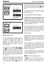
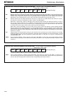
MSK3-0 Mask Alarm Bits 3-0. These bits mask the specific interrupt source bits. MSK3 masks PPCE, MSK2 masks RXPAA,
etc. If MSKn is set HIGH, the corresponding interrupt source is enabled, and the IRQ pin will respond to that interrupt
source; if set LOW, the corresponding interrupt source is masked. When masked, an interrupt source will not assert
the IRQ pin, but will still set the ALS register bit. On system power-up, all interrupts are masked. Writes to the ALS
register clear the low nibble (interrupt source bits) regardless of the data written.
PPCE Parallel Port Frame Counter Error. Used in all timing modes. The PPCE bit goes HIGH whenever there is an incorrect
number of PCKR clock cycles between PPFRi frame sync signals on the Receive parallel port. The numbers of clock
cycles expected depends on the parallel port rate selected in the IMS Register (2430, 2048, or 810 clock cycles).
The absence of PPFRi for one or more frames will not cause an interrupt (allowing free-run operation), but the PPCE
bit will go HIGH if PPFRi occurs anywhere but on an expected frame boundary.
RXPAA RX Phase Alignment Alarm. Used in TM2 operation, when INTCLK = 0. The RXPAA bit goes HIGH whenever the C4/8 input
reference goes out of phase relative to the parallel port clock (PCKR). A rising edge on the RXPAA bit indicates that the
MT90840 has adjusted the position of F0o and SPCKo, and a data slip at the serial port has occurred. Note that a
CPU write to the RPCM memory as RXPAA goes HIGH (in TM2) may be corrupted. In TM2 with SFDI = 1, a rising edge
on the RXPAA bit indicates that the F0i input is out of phase with PPFRi, implying a failure in the timing supplied by
the controlling (TM2 with SFDI = 0) MT90840. When not in TM2 the RXPAA bit may be continuously asserted, and
therefore should be masked by setting MSK2 LOW, and ignored.
TXPAA TX Phase Alignment Alarm. Used in TM1 operation. The TXPAA bit goes HIGH whenever the PCKT clock input goes
out of phase relative to the C4/8 clock. A rising edge on the TXPAA bit indicates that the MT90840 has adjusted the
position of PPFTo, and a data slip at the TX parallel port output has occurred. Note that a CPU write to the TPCM
memory as TXPAA goes HIGH (in TM1) may be corrupted. In TM1 with PFDI = 1, a rising edge on the TXPAA bit
indicates that the PPFTi input is out of phase with F0i, implying a failure in the timing supplied by the controlling
(TM1 with PFDI=0) MT90840.
FSA Frame Slip on Elastic Buffer. Used in TM1 operation. The FSA bit goes HIGH when either an overflow or underun
condition on the Receive parallel port’s elastic buffer has been detected. A rising edge on the FSA bit indicates that
a frame of data from the RX parallel port has been dropped, or repeated. In TM2, TM3, and TM4 the user should
mask this bit by setting MSK0 LOW.
Note: The interrupt source bits are latched, and remain high until cleared by the CPU. The interrupt source bits (ALS low
nibble) are cleared by writing the mask bits (ALS high nibble), regardless of the data written.
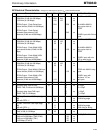
Alarm Status Register (ALS) - READ/WRITE
76543210
MSK2 MSK1 MSK0 PPCE TXPAAMSK3 RXPAA FSA