


Preliminary Information MT90840
2-255
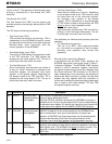
Test Data Registers
As specified in the IEEE 1149.1 Standard, the
MT90840 JTAG interface contains two test data
registers:
• The Boundary Scan Register consists of a
series of Boundary-Scan Cells arranged to form
a scan path around the boundary of the core
logic of the MT90840.
• The Bypass Register is a single stage
shift-register that provides a one-bit path that
minimizes the distance for test data shifting
from the MT90840’s TDI to its TDO.
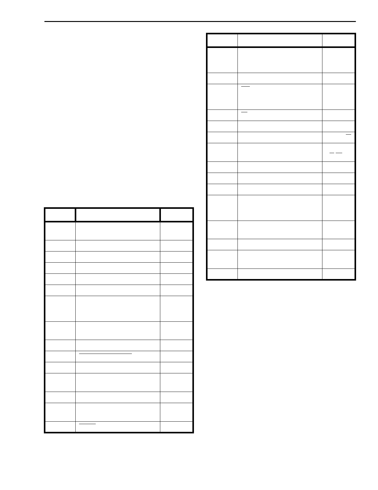
The MT90840 Boundary-Scan register contains 107
bits. The suffix (‘in’, ‘out’, or ‘en’) indicates the nature
and direction of the BSC. Bit 1 in Table 4 is the first
bit clocked out. All tristate enable bits are asserted
HIGH (i.e. a logic 1 enables the corresponding group
of output/bidirectional pins). Note that clocking all
zeros into the scan path register will set all outputs to
tristate (outputs disabled).
Please visit our web site at www.semicon.mitel.com
to download a BSDL file for the MT90840.
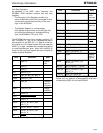
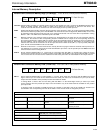
Cells Definition Note
1 ppfri_in first bit
out
2 pckt_in
3 pckr_in
4:11 pdi<0:7>_in
12:14 ppft_en, ppft_out, ppft_in
15:22 pdo<0:7>_out
23 pdo_en enables
pdo<0:7
>outputs
24:27 cto<0:3>_out always
enabled
28 c48r2_in
29:31 f0_en, f0_out, f0_in
32 c48r1_in
33:35 sti<7>_en, sti<7>_out,
sti<7>_in
36:53 sti<6>, sti<5>, ... sti<1>
54:56 sti<0>_en, sti<0>_out,
sti<0>_in
57 res_in
Table 4 - Boundary-Scan Register
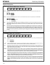
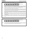
Cells Definitions Note
58 irq_en tied
HIGH
internally
59 irq_out
60 dta_out ‘pseudo’
open-dra
in
61 cs_in
62 asale_in
63 dsrdb_in pin: ds/rd
64 wrb_in pin:
r/w\wr
65:66 ad<7>_out, ad<7>_in
67:78 ad<6>, ad<5>, ... ad<1>
79:80 ad<0>_out, ad<0>_in
81 ad_en enables
ad<0:7>
outputs
82:84 sto<0>_en, sto<0>_out,
sto<0>_in
85:102 sto<1>, sto<2>, ... sto<6>
103:105 sto<7>_en, sto<7>_out,
sto<7>_in
106:107 spcko_en, spcko_out
Table 4 - Boundary Scan Register