


MT90840 Preliminary Information
2-258
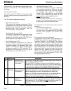
This register selects which 128 byte page of which internal memory will be accessed by the CPU when the address bit AD<7>
is high. (When address bit AD<7> is low, the control registers are accessed.)
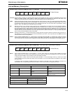
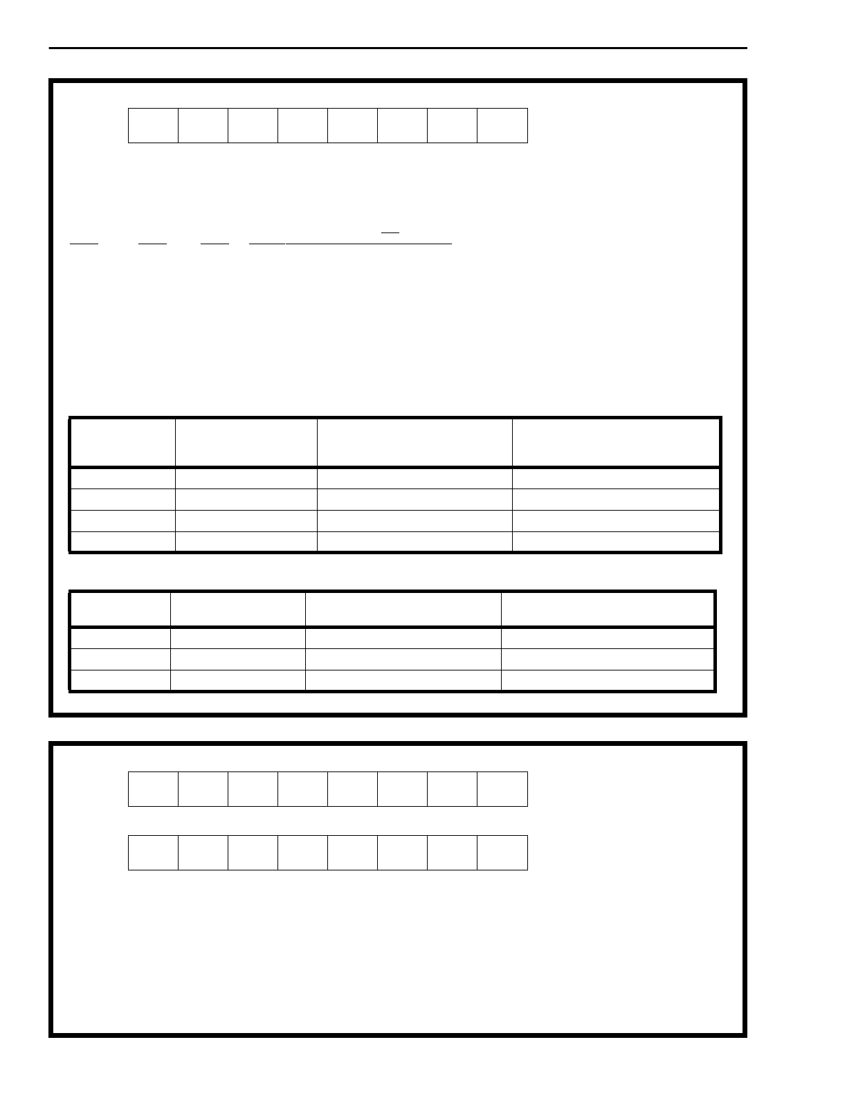
SEL2-0 Memory Select bits. Used by the CPU to select the internal memories of the MT90840 for read or write operations.
SEL2-0 bits have to be written before any READ/WRITE operation is performed on the internal memories.
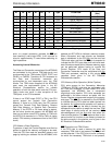
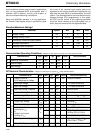
SEL2 SEL1 SEL0 Memory Selected for RD/WR operation
0 0 0 Receive Path Connection Memory Low (RPCM Low)
0 0 1 Receive Path Connection Memory High (RPCM High)
0 1 0 Receive Path Data Memory (RPDM)
0 1 1 Enable Memory Block-Programming feature for RPCM High
1 0 0 Transmit Path Connection Memory Low (TPCM Low)
1 0 1 Transmit Path Connection Memory High (TPCM High)
1 1 0 Transmit Path Data Memory (TPDM)
1 1 1 Enable Memory Block-Programming feature for TPCM High
HA11-7 High Address Bits 11-7. These bits select which 128 byte page of the selected memory (see SEL2-0 bits) will be
accessed by the CPU. Used along with AD0-AD6 input lines to address the MT90840 internal memories when the
address bit AD<7> is high. See RPCM, TPCM, RPDM and TPDM Address Mapping section for more details.
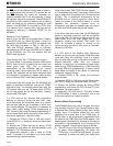
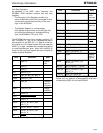
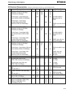
To address serial time slots in TPDM or RPCM:
To address parallel time slots in RPDM or TPCM:
Serial Port
Data Rate
Number of Serial Port
Input and Output
Streams
HA bits and input address lines, or
TPCM address bits, used to select
ST stream.
HA bits and input address lines, or
TPCM address bits, used to select the
time slot.
2 Mbps Balanced 8i x 8o (256 channels) HA7 + AD6-AD5 / AB7-AB5 AD4-AD0 / AB4-AB0 (32 time slots)
2 Mbps Add/Drop 16 i/o (512 channels) HA8-HA7 + AD6-AD5 / AB8-AB5 AD4-AD0 / AB4-AB0 (32 time slots)
4 Mbps 8i x 8o (512 channels) HA8-HA7 + AD6 / AB8-AB6 AD5-AD0 / AB5-AB0 (64 time slots)
8 Mbps 4i x 4o (512 channels) HA8-HA7 / AB8-AB7 AD6-AD0 / AB6-AB0 (128 time slots)
Parallel Port
Data Rate
Number of Channels HA bits and input address lines used
to select channel in TPCM.
RPCM address bits used to select chan-
nel.
19.44 Mbyte/s 2430 HA11-HA7 + AD6-AD0 AB11-AB0
16.384 Mbyte/s 2048 HA10-HA7 + AD6-AD0 AB10-AB0
6.480 Mbyte/s 810 HA9-HA7 + AD6-AD0 AB9-AB0
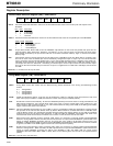
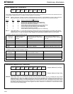
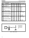
Control Register (CR) - READ/WRITE
76543210
SEL1 SEL0 HA11 HA10 HA8SEL2 HA9 HA7
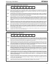
PSD10-0 Phase Status Data 10-0. The PSD bits represent the phase status of the serial port, as sampled at every second
PPFRi frame (every 250 µsec). PSD0 is the phase of the internal 4.096 MHz clock, PSD1-9 count the cycles of the
4.096 MHz within a frame, and PSD10 toggles each frame (even/odd frame bit). The PSD bits enable the CPU to
monitor the relative phases of the Receive parallel port and the serial port. This is especially useful in TM1, where
the PSD bits might be used by the CPU to monitor a PLL control loop, since the elastic buffer in the Receive parallel
port allows great variation in phase. These registers should be read twice in succession, in case the CPU access
occurs close to the sampling edge.
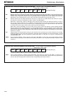
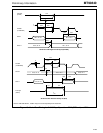
Phase Status Registers (PSD) - READ Only
76543210
PSD6 PSD5 PSD4 PSD3 PSD1PSD7 PSD2 PSD0
76543210
0
0 0 0 0 PSD9PSD10 PSD8
Register Address 8 (Low Byte)
Register Address 9 (High 3-bits)