


MT90840 Preliminary Information
2-244
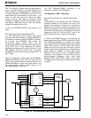
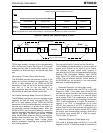
Timing Mode 3 (TM3) - Bus Slave
Synchronous Parallel Port With ST-BUS Clock
Slave
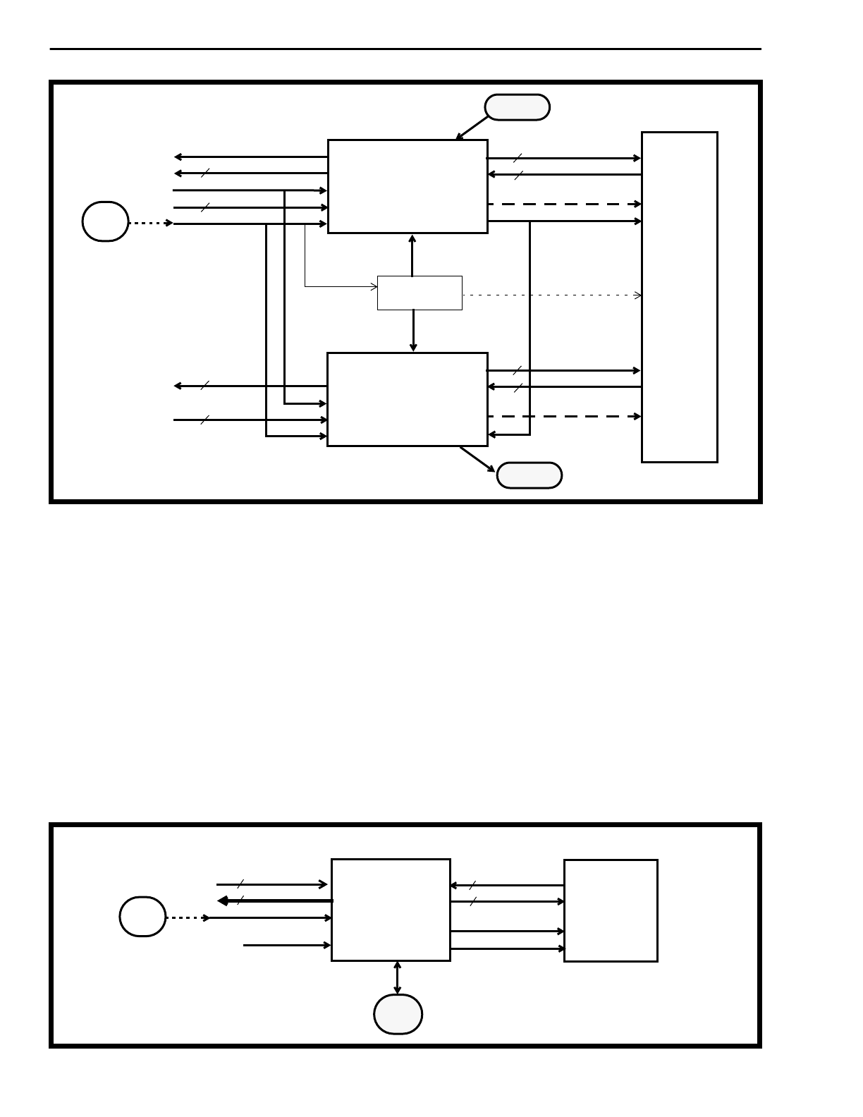
Timing Mode 3 is used where the main TDM clock ref-
erence resides on the parallel port side of the system,
and where the receive parallel port and the transmit
parallel port are aligned. (An example is a node on a
backplane.) Timing on the serial port is tightly tied to
the receive parallel port, and the transmit parallel
port is clocked by the receive parallel port clock. In
TM3, PCKT and PPFTo are not used. See Figure 7
for a connection example.
In TM3, the MT90840 timing is controlled by the
parallel port frame pulse (PPFRi) and clock (PCKR).
The MT90840 generates the serial port output frame
pulse (F0o) locked to PPFRi. TM3 is similar to TM2
with two main differences: the parallel Bypass Path is
disabled, and the parallel port receive and transmit
buses are synchronized and both aligned with
PPFRi. A fixed offset exists between F0o and PPFRi
due to serial-to-parallel conversion. The MT90840
will align F0o so that it proceeds PPFRi by 3.8 µsec.
In TM3 the internal clock divider circuit is always
enabled, regardless of the state of the INTCLK bit
(C4/8R1 and C4/8R2 are unused). Therefore TM3 is
limited to 19.44 and 16.384 Mbyte/s parallel port
rates, and 2.048 and 4.096 Mbps serial port rates.
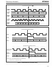
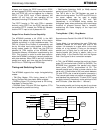
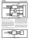
Figure 6b - TM2 Multiple-MT90840 Configuration
8
8
8 kHz TX
Data TX
8 kHz RX
Data RX
PCKR
PPFT
PDo0-7
PDi0-7
PPFRi
STi0-7
STo0-7
SPCKo
F0o
8
STi/o 0-7
8
STi/o 0-7
8 kHz
4.096 MHz
MT90840
CPU
TX/RX Clock
C4/8R1 & 2
PLL
4.096 MHz or
8.192 MHz
ST-BUS
Components
8 kHz
Source
(8.192 MHz)
8
8
Data TX
Data RX
PCKR
PPFT
PDo0-7
PDi0-7
PPFRi
STi0-7
STo0-7
SPCKo
F0i
8
STi/o 0-7
8
STi/o 0-7
4.096 MHz
MT90840
CPU
C4/8R1 & 2
SFDI = 1
SFDI = 0
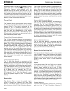
Figure 7 - Timing Mode 3 Configuration
8
8
Aligned
RX/TX Clock
8 kHz REF
PDi0-7
PDo0-7
PPFRi
PCKR
STi0-7
STo0-7
SPCKo
F0o
8
STi/o 0-7
8
STi/o 0-7
4.096 MHz
MT90840
CPU
ST-BUS
Components
Frames
8 kHz
Source
8 kHz