


Preliminary Information MT90840
2-251
short, or a signal contention, prevents the DTA pin
from reaching a valid logic HIGH, it will continue to
drive for approximately 15 nsec before switching to
high-impedance.
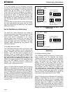
Accessing Internal Memories
The Data and Connection memories of the MT90840
are connected to the various TDM data ports, and
synchronized to the TDM clocks (PCKR, PCKT, and
C4/8R1 or C4/8R2). Therefore all CPU accesses to
the Data and Connection memories are
synchronized to, and dependent upon, the TDM
clocks. The TDM clocks supplied to the MT90840
must meet the requirements given in the AC
Electrical Characteristics section for reliable
operation of both the data switch and the CPU port.
Faulty clocks can result in data corruption at the
TDM ports, or on CPU accesses.
If there is no PCKR clock (PCKT in TM1), the CPU
cannot access the Transmit Path Connection
Memory. If there is no C4/8 clock, the CPU cannot
access the Transmit Path Data Memory, Receive
Path Data Memory, or Receive Path Connection
Memory. If the PPFRi or F0 frame pulse is absent,
but the other clocks are present, the MT90840 will
free-run and allow normal CPU access. (In TM2 with
the INTCLK bit asserted, or in TM3 or TM4, all clocks
and all CPU memory accesses are tied to the PCKR
clock.)
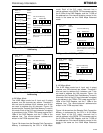
CPU Memory Read Operation
To perform a read, the Control Register must first be
written to specify the memory and page to be read.
Then the CPU can read the specified memory and
page by latching an address into the MT90840, with
address pin AD7 HIGH to indicate a memory access.
When chip-select and read signals are asserted,
data is transferred to the CPU port on the next free
TDM clock edge, and then the DTA pin is asserted to
indicate that the CPU port data pins hold valid read-
data. Numerous reads within the same memory page
can be performed without having to re-write the
Control Register. CPU reads of the Data and
Connection memories must be multiplexed with the
TDM port accesses, resulting in the varying DTA
response times given in the AC Electrical
Characteristics section.
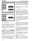
CPU Memory Write Operation (Write Pipeline)
CPU write access to the Connection Memories
(TPCM and RPCM) must also be multiplexed with
the TDM port accesses. To allow faster CPU write
operations, the MT90840 has a transparent
single-byte write pipeline. CPU write accesses are
performed in the same manner as reads, with the
Control Register programmed to specify the memory
and page. The DTA pin is asserted by the MT90840
to indicate that the CPU data has been latched into
the device. An isolated write operation will receive a
register-speed DTA, as the data is latched into the
transparent write pipeline to await the next free TDM
clock edge. A second write will not receive a DTA
acknowledgment until the first write has exited the
internal write pipeline. The DTA response time on the
second write is a function of the memory chosen for
the write currently in the pipeline, and is given in the
AC Electrical Characteristics section.
DTA Operation and TDM Clocks
If the CPU tries to read a memory for which the
necessary TDM clock is not present, the DTA pin will
not be asserted. If the CPU tries to write a memory
for which the necessary TDM clock is not present,
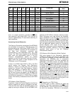
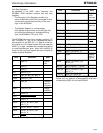
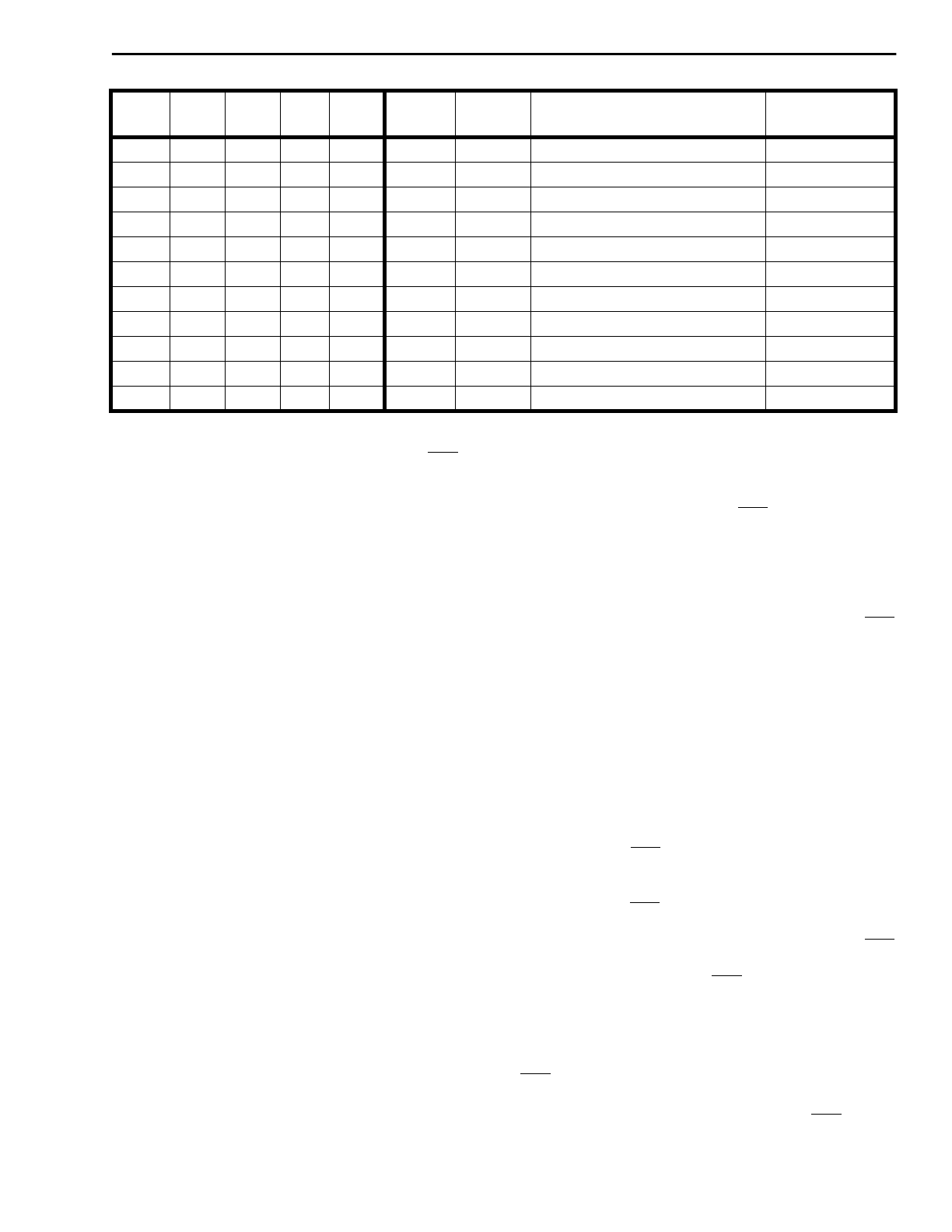
Table 2 - MT90840 Register Address Mapping
A7 A3 A2 A1 A0 # Type LOCATION
Reset Value
(Hex)
0 0 0 0 0 0 R/W IMS Register 60
0 0 0 0 1 1 R/W Control Register 00
0 0 0 1 0 2 R/W TIM Register 00
0 0 0 1 1 3 R/W GPM Register 00
0 0 1 0 0 4 R/W ALS Register 0X
0 0 1 0 1 5 R/W Test (leave 00hx) 00
0 0 1 1 0 6 - reserved
0 0 1 1 1 7 - reserved
0 1 0 0 0 8 RO Phase Status (Low byte) XX
0 1 0 0 1 9 RO Phase Status (High 3 bits) 0X
0 1 0 1 0 10 - reserved