Preliminary Information MT90840
2-245
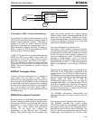
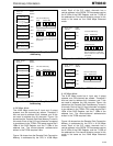
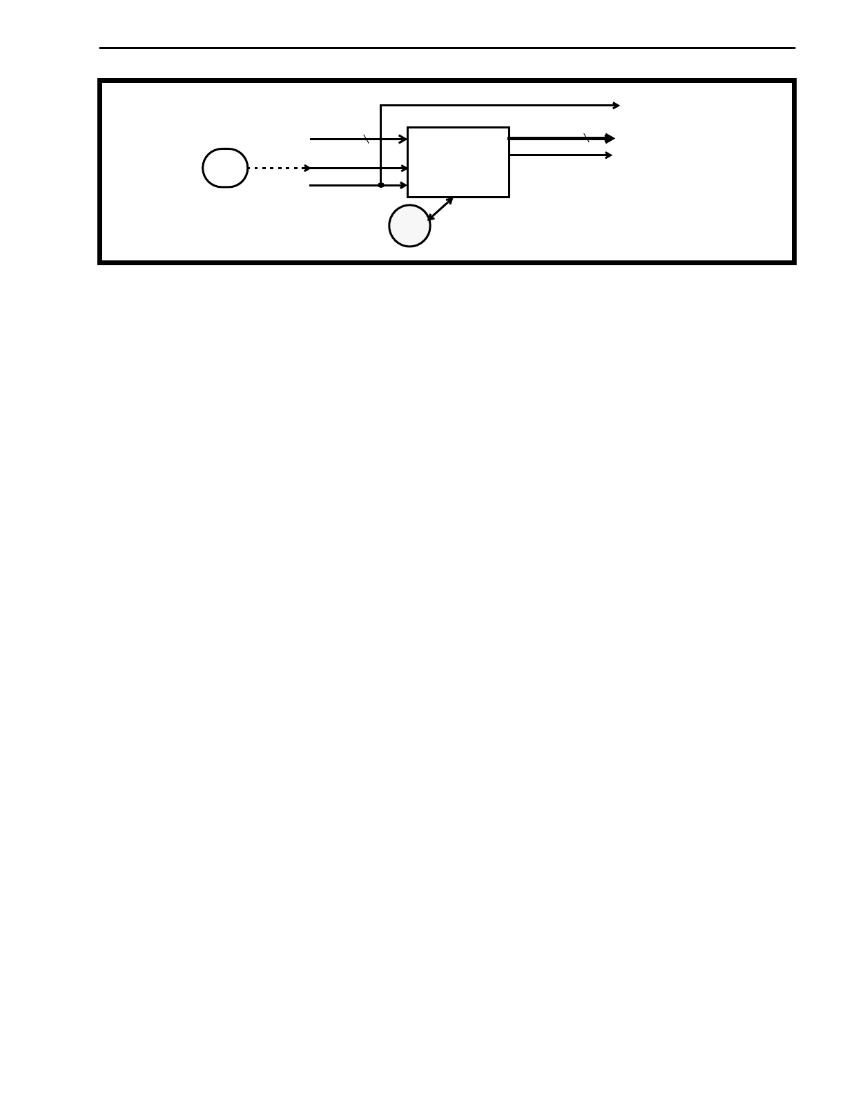
Timing Mode 4 (TM4) - Parallel Data Switching
Timing Mode 4 is used to provide switching of up to
2430 parallel input channels to the same number of
parallel output channels. Parallel TDM data is
clocked in at PDi0-7 by PCKR, framed by PPFRi.
Switching is performed as programmed in the Tx
Path Connection Memory, and data is output on
PDo0-7, framed by PPFTo and clocked by PCKR.
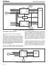
See Figure 8 for connection details.
In TM4, PPFTo and PDo0-7 are offset (delayed) from
PPFRi and PDi0-7 by a fixed 4 clock cycles (3.5
clock cycles if the TCP bit is high). All the serial port
data and timing signals, and PCKT, are unused in
TM4. The internal clock divider is used to generate
an internal C4 clock to allow CPU reads from the
RPDM. TM4 is only available for 19.44 and 16.384
Mbyte/s rates.
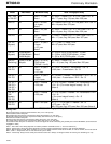
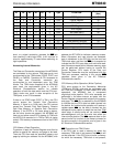
MT90840 Throughput Delay
In many isochronous applications it is important to
know and/or limit the delay of data. Table 1
summarizes the data throughput delay values for all
timing modes of the MT90840. It is worth noting that
the worst-case “round-trip” delays are not as large as
the sum of the worst-case delays on the individual
links. This is shown by the last 5 rows of Table 1,
which give the delays for some representative two
MT90840 setups.
MT90840 Per-channel Functions
Several functions of the MT90840 are programmable
for each individual parallel channel or serial channel.
Per-channel functions on the parallel port side are
programmed in the Transmit Path Connection
Memory High (TPCM High), and per-channel
functions on the serial port interface are
programmed in the Receive Path Connection
Memory High (RPCM High). On the parallel port
these per-channel features are Bypass, Control
Outputs, Output Enable, and Message Mode. On the
serial port the per-channel features are Output
Enable, Message Mode and Direction Control. These
functions are generally available in all of the data
rates and timing/switching modes.
Per-channel Bypass on the Parallel Port
This feature, when enabled, causes the specific
individual parallel output channel at PDo to transmit
the data received at the same number input channel
at PDi. This can be used to perform a bypass (on a
ring) or a loopback (in a star). This feature is only
provided in Timing Modes 1 and 2. In TM2 the
data-delay from PDi to PDo is fixed (as is the delay
between PPFRi and PPFT). In TM1 the data-delay is
elastic (and dependent on the timing of PPFRi and
F0i).
The per-channel bypass feature is controlled by the
PPBY bits of the TPCM High as explained in the
register section. If the PPBY bit is HIGH at a specific
TPCM address, the corresponding parallel output will
transmit the data received in the corresponding input
channel. When the PPBY bit is LOW, the
corresponding output channel can be used for
message-mode data, or for switched-data from the
serial port. A bypass input channel is still copied to
the Receive Path Data Memory, and may also be
switched to the serial port, or read by the CPU from
the Receive Path Data Memory.
The MT90840 per-channel output-enable and
message-mode bits have higher priority than the
PPBY bit.
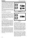
Per-channel Control Outputs on the Parallel Port
The MT90840 provides four control outputs
(CTo0-CTo3) which are synchronized to the parallel
port output timing. Each of the CTo output pins is
controlled by the CT0-3 bits of the TPCM High. (The
CTo0 pin and bit are programmed with the Output
Enable data.) The contents of the CTo bit in each
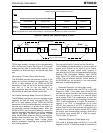
Figure 8 - Timing Mode 4 Configuration
8
TX 8 kHz REF
PDo0-7
PPFTo
PDi0-7
PCKR
PPFRi
8
8 kHz RX
CPU
19.44 or 16.384 MHz (RX)
Clock Reference
Parallel Data In
MT90840
Parallel Data Out
8 kHz
Source


