8XC196NP, 80C196NU USER’S MANUAL
2-8
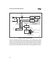
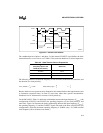
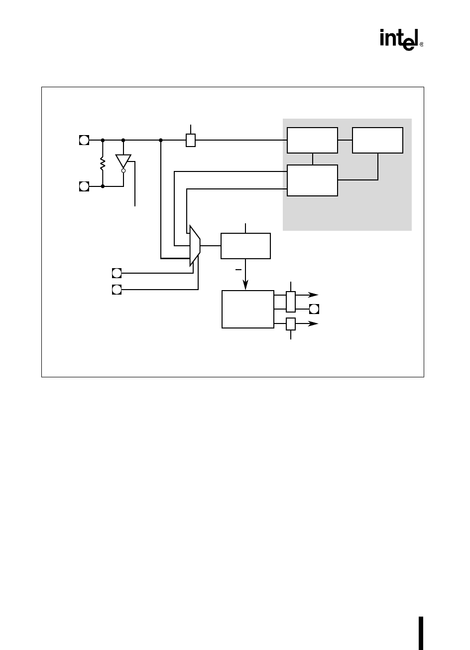
Figure 2-4. Clock Circuitry (80C196NU)
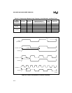
For both the 8XC196NP and 80C196NU, the rising edges of PH1 and PH2 generate CLKOUT
(Figure 2-5). The clock circuitry routes separate internal clock signals to the CPU and the periph-
erals to provide flexibility in power management. (“Reducing Power Consumption” on page 12-3
describes the power management modes.) It also outputs the CLKOUT signal on the CLKOUT
pin. Because of the complex logic in the clock circuitry, the signal on the CLKOUT pin is a de-
layed version of the internal CLKOUT signal. This delay varies with temperature and voltage.
A3063-02
Clock
Generators
CPU Clocks (PH1, PH2)
Divide-by-two
Circuit
PLLEN1
Phase-locked Loop
Clock Multiplier
Phase
Comparator
Filter
Phase-
locked
Oscillator
PLLEN2
Disable
PLL
(Powerdown)
Peripheral Clocks (PH1, PH2)
CLKOUT
Disable Clocks
(Standby, Powerdown)
Disable Clocks
(Idle, Standby, Powerdown)
XTAL1
XTAL2
F
XTAL1
Disable
Oscillator
(Powerdown)
Disable Clock Input
(Powerdown)
f
F
XTAL1
2F
XTAL1
4F
XTAL1
f
2


