13-21
INTERFACING WITH EXTERNAL MEMORY
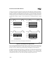
In multiplexed mode, with the full address on the bus for only half of the cycle, the external de-
vice has less time to receive it and to respond. As a result, for the same bus-cycle length (4t)
a
multiplexed system requires a faster external device (unless wait states are added to the bus cy-
cle). Although the multiplexed mode has this disadvantage, it is useful for compatibility with de-
vices designed for multiplexed operation.
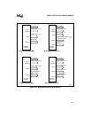
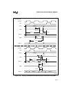
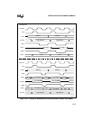
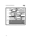
In a 16-bit system (left side of Figure 13-8 and Figure 13-9) one data word can be transferred over
AD15:0 in a single bus cycle. In an 8-bit system, one data word is transferred as two bytes over
AD7:0 in successive bus cycles, and AD15:8 drive the upper eight address bits for the entire bus
cycle.
The flexibility of the chip-select unit enables you to specify the bus width, the number of wait
states, and a multiplexed or demultiplexed bus for each of the six chip-select outputs. The system
in Figure 13-5 on page 13-13 illustrates a mixture of 8-bit and 16-bit devices with different num-
bers of wait states.
13.5.1 A 16-bit Example System
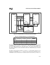
Figure 13-10 shows a 16-bit system in demultiplexed mode. The flash memory receives the ad-
dress on A18:1; data is transferred on AD15:0. Using the WR# signal as shown, this system
writes words and not single bytes to the memory. (Using WRL# and WRH#, you can write single
bytes on a 16-bit bus.


