13-27
INTERFACING WITH EXTERNAL MEMORY
When selecting infinite wait states, be sure to add external hardware to count wait states and re-
lease READY within a specified period of time. Otherwise, a defective external device could tie
up the address/data bus indefinitely.
NOTE
Ready control is valid only for external memory; you cannot add wait states
when accessing internal ROM.
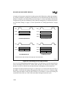
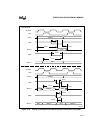
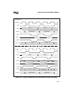
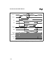
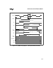
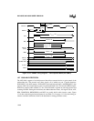
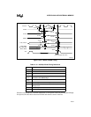
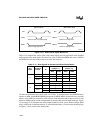
Setup and hold timings must be met when using the READY signal to insert wait states into a bus
cycle (see Table 13-11 and Figures 13-13 through 13-15). Because a decoded, valid address is
used to generate the READY signal, the setup time is specified relative to the address being valid.
This specification, T
AVYV
, indicates how much time the external device has to decode the address
and assert READY after the address is valid. The READY signal must be held valid until the
T
CLYX
timing specification is met. Typically, this is a minimum of 0 ns from the time CLKOUT
goes low. Do not exceed the maximum T
CLYX
specification or additional (unwanted) wait states
might be added. In all cases, refer to the datasheets for the current specifications for T
AVYV
and
T
CLYX
.
.
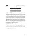
Table 13-11. READY Signal Timing Definitions
Symbol Definition
T
AVDV
Address Valid to Input Data Valid
Maximum time the memory device has to output valid data after the device outputs a valid
address.
T
AVYV
Address Valid to READY Setup
Maximum time the memory system has to assert READY after the device outputs the address
to guarantee that at least one wait state will occur.
T
CHYX
READY Hold after CLKOUT High
If maximum specification is exceeded, additional wait states will occur.
T
CLYX
READY Hold after CLKOUT Low
Minimum hold time is always 0 ns. If maximum specification is exceeded, additional wait
states will occur.
T
LHLH
ALE Cycle Time
Minimum time between ALE pulses.
T
RLDV
RD# Low to Input Data Valid
Maximum time the memory system has to output valid data after the device asserts RD#.
T
RLRH
RD# Low to RD# High
RD# pulse width.
T
QVWH
Data Valid to WR# High
Time between data being valid on the bus and WR# going inactive. Memory devices must
meet this specification.
T
WLWH
WR# Low to WR# High
WR# pulse width.


