8-4
8XC196NP, 80C196NU USER’S MANUAL
8.3 SERIAL PORT MODES
The serial port has both synchronous and asynchronous operating modes for transmission and re-
ception. This section describes the operation of each mode.
8.3.1 Synchronous Mode (Mode 0)
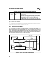
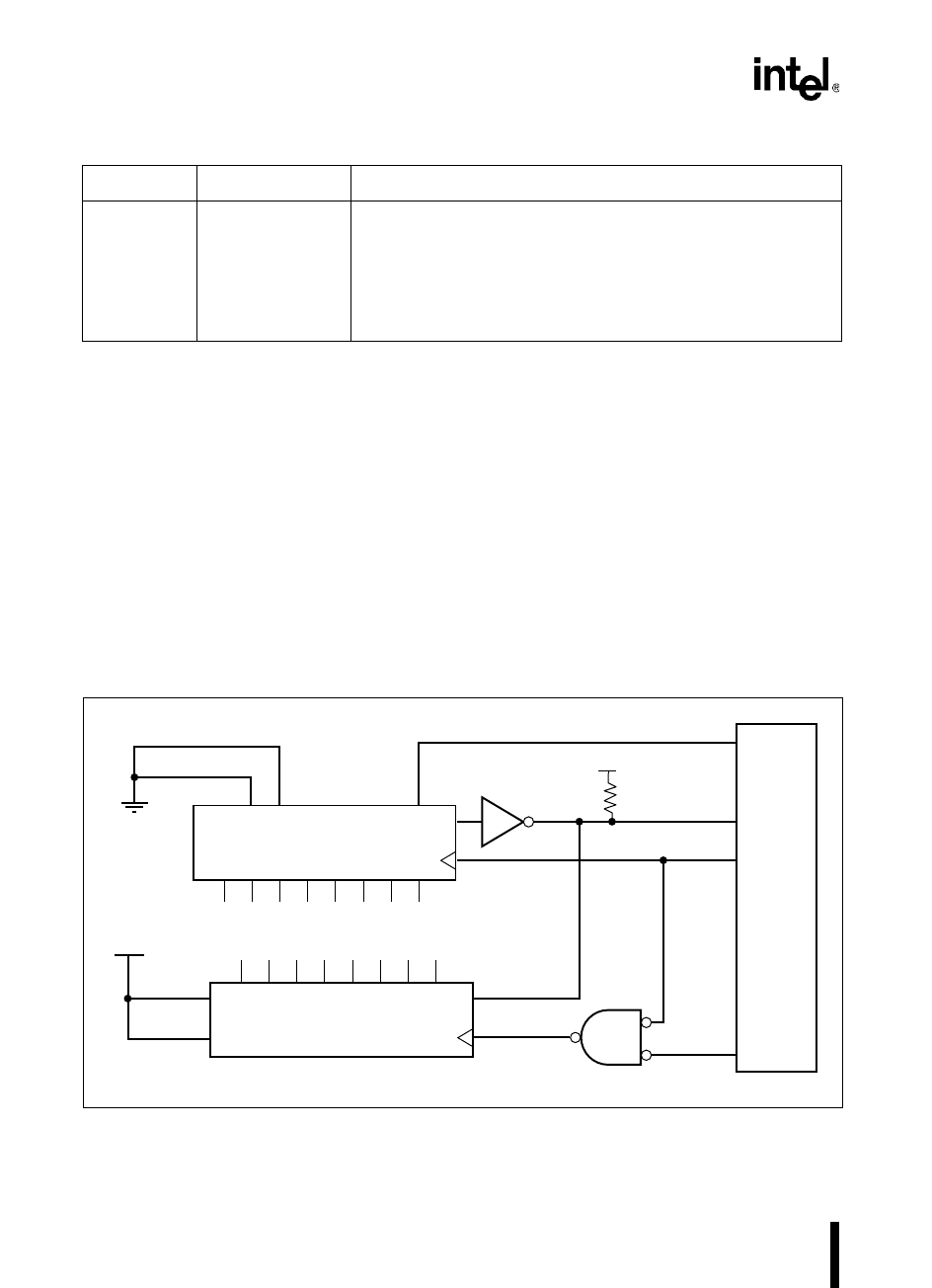
The most common use of mode 0, the synchronous mode, is to expand the I/O capability of the
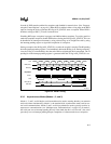
device with shift registers (see Figure 8-2). In this mode, the TXD pin outputs a set of eight clock
pulses, while the RXD pin either transmits or receives data. Data is transferred eight bits at a time
with the least-significant bit first. Figure 8-3 shows a diagram of the relative timing of these sig-
nals. Note that only mode 0 uses RXD as an open-drain output.
Figure 8-2. Typical Shift Register Circuit for Mode 0
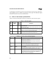
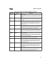
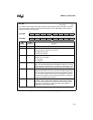
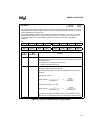
SP_STATUS 1FB9H Serial Port Status
This register contains the serial port status bits. It has status bits for
receive overrun errors (OE), transmit buffer empty (TXE), framing
errors (FE), transmit interrupt (TI), receive interrupt (RI), and
received parity error (RPE) or received bit 8 (RB8). Reading
SP_STATUS clears all bits except TXE; writing a byte to SBUF_TX
clears the TXE bit.
Table 8-2. Serial Port Control and Status Registers (Continued)
Mnemonic Address Description
Clock Inhibit
Serial In
Shift / LOAD#
P
x
.
x
RXD
TXD
8XC196
Device
Shift Register
74HC165
Shift Register
74HC164
Inputs
Outputs
Serial
In B
Clear
P
x
.
x
Clock
Serial In A
V
CC
Enable#
Clock
Data
15KΩ
74HC05
Q#
A0264-02
V
CC


