8XC196NP, 80C196NU USER’S MANUAL
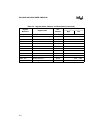
C-12
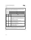
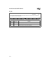
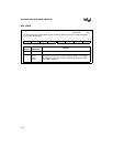
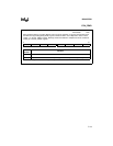
CCR1
CCR1
no direct access
†
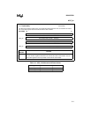
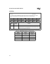
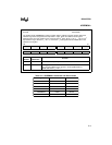
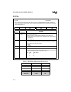
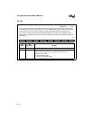
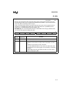
The chip configuration 1 (CCR1) register selects the 16-bit or 24-bit addressing mode and (for the
8XC196NP only) controls whether the internal ROM is mapped into two address ranges, FF2000–
FF2FFFH and 002000–002FFFH, or into FF2000–FF2FFFH only.
7 0
8XC196NP
1 101 1 REMAP MODE64 —
7 0
80C196NU
1 1DM1 1—MODE64 —
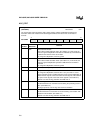
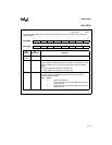
Bit
Number
Bit
Mnemonic
Function
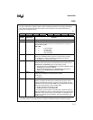
7:6 1 To guarantee device operation, write ones to these bits.
5
††
DM Deferred Mode
Enables the deferred bus-cycle mode. If the 80C196NU is using a demulti-
plexed bus and deferred mode is enabled, a delay of 2t occurs in the first
bus cycle following a chip-select output change and the first write cycle
following a read cycle. (See “Deferred Bus-cycle Mode (80C196NU Only)”
on page 13-40.)
0 = deferred bus-cycle mode disabled
1 = deferred bus-cycle mode enabled
4:3 1 To guarantee device operation, write ones to these bits.
2
††
REMAP Internal ROM Mapping
Controls the internal ROM mapping.
0 = ROM maps to FF2000–FF2FFFH only
1 = ROM maps to FF2000–FF2FFFH and 002000–002FFFH
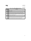
1 MODE64 Addressing Mode
Selects 64-Kbyte or 1-Mbyte addressing.
0 = selects 1-Mbyte addressing
1 = selects 64-Kbyte addressing
0 — Reserved; for compatibility with future devices, write zero to this bit.
†
The CCRs are loaded with the contents of the chip configuration bytes (CCBs) after a device reset.
The CCBs reside in nonvolatile memory at addresses FF2018H (CCB0) and FF201AH (CCB1).
††
Bit 5 is reserved on the 8XC196NP device and bit 2 is reserved on the 80C196NU device. For
compatibility with future devices, write zeros to these bits.


