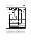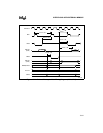
13-43
INTERFACING WITH EXTERNAL MEMORY
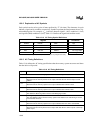
The 8XC196N
x
Meets These Specifications
f Operating frequency
Frequency of the signal input on the XTAL1 pin times the clock multiplier (
x
). For the
8XC196NP,
x
is always 1; for the 80C196NU,
x
is 1, 2, or 4, depending on the clock mode. The
internal bus speed of the device is ½ f.
t Operating period (1/f)
All AC Timings are referenced to t.
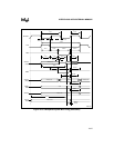
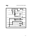
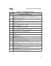
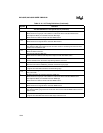
T
AVLL
Address Setup to ALE Low
Length of time ADDRESS is valid before ALE falls. Use this specification when designing the
external latch.
T
AVRL
Address Setup to RD# Low
Length of time ADDRESS is valid before RD# falls.
T
AVWL
Address Setup to WR# Low
Length of time ADDRESS is valid before WR# falls.
T
CHCL
CLKOUT High Period
Needed in systems that use CLKOUT as clock for external devices.
T
CHWL
CLKOUT High to WR# Low
Time between CLKOUT going high and WR# going active.
T
CLCL
CLKOUT Cycle Time
Normally 2t.
T
CLLH
CLKOUT Falling to ALE Rising
Use to derive other timings.
T
LHLH
ALE Cycle Time
Minimum time between ALE pulses.
T
LHLL
ALE High Period
Use this specification when designing the external latch.
T
LLAX
Address Hold after ALE Low
Length of time ADDRESS is valid after ALE falls. Use this specification when designing the
external latch.
T
LLCH
ALE Falling to CLKOUT Rising
Use to derive other timings.
T
LLRL
ALE Low to RD# Low
Length of time after ALE falls before RD# is asserted. Could be needed to ensure proper
memory decoding takes place before a device is enabled.
T
LLWL
ALE Low to WR# Low
Length of time after ALE falls before WR# is asserted. Could be needed to ensure proper
memory decoding takes place before a device is enabled.
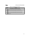
Table 13-16. AC Timing Definitions (Continued)
Symbol Definition


