


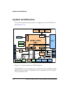
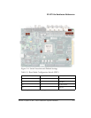

ADSP-21369 EZ-KIT Lite Evaluation System Manual 2-5
EZ-KIT Lite Hardware Reference
To use the DAI for a different purpose, disable any signal driving the DAI
pins with a switch (see “Codec Setup Switch (SW3)” on page 2-10). In
addition, the
SW3 switch allows flexible routing of the 12.288 MHz audio
oscillator’s output signal. By default, this signal is used as the master clock
(
MCLK) for the AD1835A codec.
All of the DAI signals are available externally via the expansion interface
connectors (
J3–1), as well as the 0.1” spaced header P4. The pinout of
these connectors can be found in “Schematics” on page B-1.
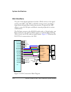
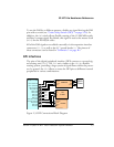
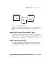
DPI Interface
The pins of the digital peripheral interface (DPI) connect to a second sig-
nal routing unit (
SRU2). The SRU2 unit, similar to the SRU, is a flexible
routing system, providing a large system of signal flows within the proces-
sor. In general, the
SRU2 allows to route the DPI pins to different internal
peripherals in various combinations.
Figure 2-3. DPI Connections Block Diagram
DPI1 (MOSI)
DPI2 (MISO)
DPI3 (SPICLK)
DPI4 (SPI_AD1835CS)
DPI5 (SPI_FLASHCS)
DPI6 (LED1)
DPI7 (LED2)
DPI8 (LED3)
DPI13 (LED4)
DPI14 (LED5)
DPI9 ( UART TX)
DPI10 (UART RX)
DPI12 (UART CTS)
DPI11 (UART RTS)
LED1
LED2
LED3
LED4
LED5
AD1835
SPI
FLASH
CLATCH
CCLK
COUT
CIN
CS/
SCK
SO
SI
ADSP -21369
T2IN
R2OUT
R1OUT
T1IN
T2OUT
R2IN
R1IN
T1OUT
ADM3202
DB-9
Conn