


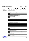
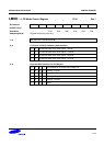
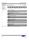

S3C8245/P8245/C8249/P8249 CONTROL REGISTER
4-15
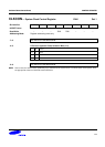
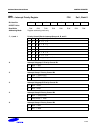
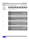
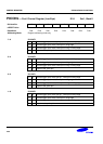
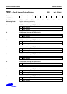
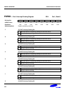
LCON — LCD Control Register D0H Set 1
Bit Identifier .7 .6 .5 .4 .3 .2 .1 .0
nRESET Value 0 0 0 0 0 0 0 0
Read/Write R/W R/W R/W R/W – R/W R/W R/W
Addressing Mode Register addressing mode only
.7 LCD Output Segment and Pin Configuration Bits
0 P5.4–P5.7 I/O is selected
1 SEG28–SEG31 is selected, P5.4–P5.7 I/O is disabled
.6 LCD Output Segment and Pin Configuration Bits
0 P5.0–P5.3 I/O is selected
1 SEG24–SEG27 is selected, P5.0–P5.3 I/O is disabled
.5 LCD Output Segment and Pin Configuration Bits
0 P4.4–P4.7 I/O is selected
1 SEG20–EG23 is selected, P4.4–P4.7 I/O is disabled
.4 LCD Output Segment and Pin Configuration Bits
0 P4.0–P4.3 I/O is selected
1 SEG16–SEG19 is selected, P4.0–P4.3 I/O is disabled
.3 Not used for the S3C8245/C8249
.2 LCD Bias Voltage Selection Bit
0 Enable LCD initial circuit (internal bias voltage)
1 Disable LCD initial circuit for external LCD driving resister (external bias voltage)
.1 Voltage Booster Enable/disable Bit
0 Stop voltage booster (Clock stop and cut off current charge path)
1 Run voltage booster (Clock run current and turn on charge path)
.0 LCD Display Control Bit
0 LCD output low; turn display off, COM and SEG output low cut off voltage booster
(Booster clock disable)