


nRESET and POWER-DOWN S3C8245/P8245/C8249/P8249
8-4
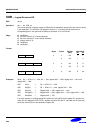
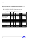
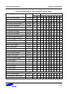
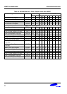
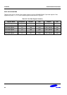
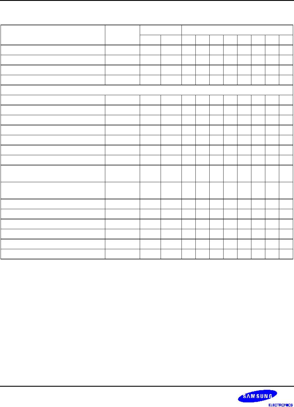
Table 8-3. S3C8245/P8245 Set 1, Bank 1 Register Values after nRESET
Register Name Mnemonic Address Bit Values after nRESET
Dec Hex 7 6 5 4 3 2 1 0
Port 4 control High register P4CONH 236 ECH 0 0 0 0 0 0 0 0
Port 4 control Low register P4CONL 237 EDH 0 0 0 0 0 0 0 0
Port 5 Control High Register P5CONH 238 EEH 0 0 0 0 0 0 0 0
Port 5 Control Low Register P5CONL 239 EFH 0 0 0 0 0 0 0 0
Locations F0H is factory use only.
Timer 0 Control Register T0CON 241 F1H 0 0 0 – 0 0 0 0
Timer 0 Counter Register (High Byte) T0CNTH 242 F2H 0 0 0 0 0 0 0 0
Timer 0 Counter Register (Low Byte) T0CNTL 243 F3H 0 0 0 0 0 0 0 0
Timer 0 Data Register (High Byte) T0DATAH 244 F4H 1 1 1 1 1 1 1 1
Timer 0 Data Register (Low Byte) T0DATAL 245 F5H 1 1 1 1 1 1 1 1
Voltage Level Detector Control Register VLDCON 246 F6H 0 0 0 0 0 0 0 0
AD Converter Control Register ADCON 247 F7H – 0 0 0 0 0 0 0
AD Converter Data Register
(High Byte)
ADDATAH 248 F8H x x x x x x x x
AD Converter Data Register
(Low Byte)
ADDATAL 249 F9H x x x x x x x x
Watch Timer Control Register WTCON 250 FAH 0 0 0 0 0 0 0 0
Timer 1 Control Register T1CON 251 FBH 0 0 0 0 0 0 0 0
Timer 1 Counter Register (High Byte) T1CNTH 252 FCH 0 0 0 0 0 0 0 0
Timer 1 Counter Register (Low Byte) T1CNTL 253 FDH 0 0 0 0 0 0 0 0
Timer 1 Data Register (High Byte) T1DATAH 254 FEH 1 1 1 1 1 1 1 1
Timer 1 Data Register (Low Byte) T1DATAL 255 FFH 1 1 1 1 1 1 1 1