


S3C8245/P8245/C8249/P8249 A/D CONVERTER
15-3
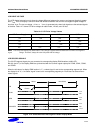
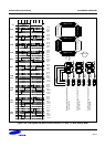
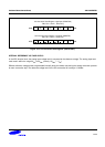
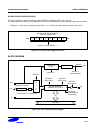
A/D Converter Data Register, High Byte (ADDATAH)
F8H, Set 1, Bank 1, Read Only
.7 .6 .5 .4 .3 .2 .1 .0MSB LSB
A/D Converter Data Register, Low Byte (ADDATAL)
F9H, Set 1, Bank 1, Read Only
.1 .0MSB LSB
Figure 15-2. A/D Converter Data Register (ADDATAH/L)
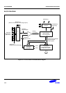
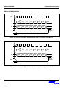
INTERNAL REFERENCE VOLTAGE LEVELS
In the ADC function block, the analog input voltage level is compared to the reference voltage. The analog input level
must remain within the range AV
SS
to AV
REF
(usually, AV
REF
= V
DD
).
Different reference voltage levels are generated internally along the resistor tree during the analog conversion process
for each conversion step. The reference voltage level for the first conversion bit is always 1/2 AV
REF
.