S3C8245/P8245/C8249/P8249 ELECTRICAL DATA
19-13
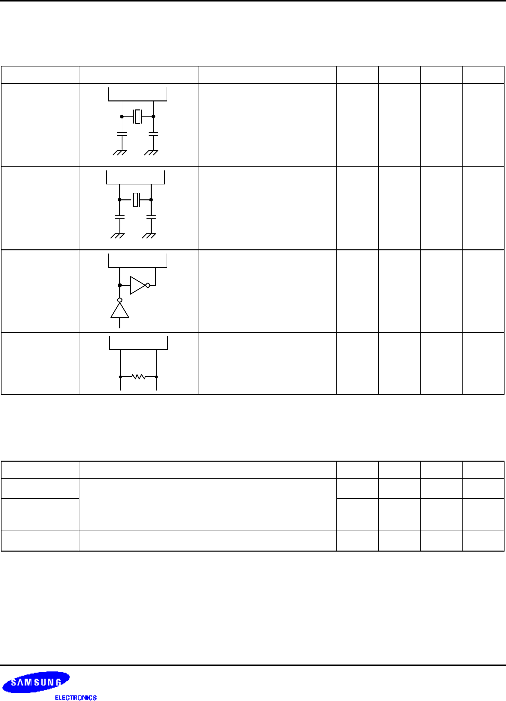
Table 19-11. Main Oscillator Frequency (f
OSC1
)
(T
A
= -25
°
C to +85
°
C, V
DD
= 1.8 V to 5.5 V)
Oscillator Clock Circuit Test Condition Min Typ Max Unit
Crystal
X
IN
C1 C2
X
OUT
Crystal oscillation frequency 1 – 10 MHz
Ceramic
X
IN
C1 C2
X
OUT
Ceramic oscillation frequency 1 – 10 MHz
External clock
X
IN
X
OUT
X
IN
input frequency 1 – 10 MHz
RC
X
IN
X
OUT
R
V
DD
= 5 V 1 – 2 MHz
Table 19-12. Main Oscillator Clock Stabilization Time (t
ST1
)
(T
A
= -25
°
C to +85
°
C, V
DD
= 2.0 V to 5.5 V)
Oscillator Test Condition Min Typ Max Unit
Crystal V
DD
= 2.0 V to 5.5 V – – 40 ms
Ceramic Stabilization occurs when V
DD
is equal to the minimum
oscillator voltage range.
– – 4 ms
External clock X
IN
input high and low level width (t
XH
, t
XL
) 50 – 500 ns
NOTE: Oscillation stabilization time (t
ST1
) is the time required for the CPU clock to return to its normal oscillation
frequency after a power-on occurs, or when Stop mode is ended by a nRESET signal.
The nRESET should therefore be held at low level until the t
ST1
time has elapsed


