


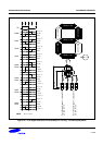
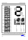

S3C8245/P8245/C8249/P8249 LCD CONTROLLER/DRIVER
14-3
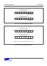
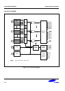
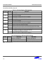
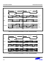
LCD RAM ADDRESS AREA
RAM addresses 00H - 0FH of page 4, or page 2, according to ROM size, are used as LCD data memory. When the
bit value of a display segment is "1", the LCD display is turned on; when the bit value is "0", the display is turned off.
Display RAM data are sent out through segment pins SEG0–SEG31 using a direct memory access (DMA) method
that is synchronized with the f
LCD
signal. RAM addresses in this location that are not used for LCD display can be
allocated to general-purpose use.
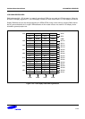
SEG0
BIT.7
BIT.3
BIT.7
BIT.3
BIT.7
BIT.3
BIT.7
BIT.3
BIT.7
BIT.3
BIT.3
BIT.7
BIT.3
BIT.7
BIT.3
BIT.7
BIT.3
BIT.7
BIT.6
BIT.2
BIT.6
BIT.2
BIT.6
BIT.2
BIT.6
BIT.2
BIT.6
BIT.2
BIT.2
BIT.6
BIT.2
BIT.6
BIT.2
BIT.6
BIT.2
BIT.6
BIT.5
BIT.1
BIT.5
BIT.1
BIT.5
BIT.1
BIT.5
BIT.1
BIT.5
BIT.1
BIT.1
BIT.5
BIT.1
BIT.5
BIT.1
BIT.5
BIT.1
BIT.5
BIT.4
BIT.0
BIT.4
BIT.0
BIT.4
BIT.0
BIT.4
BIT.0
BIT.4
BIT.0
BIT.0
BIT.4
BIT.0
BIT.4
BIT.0
BIT.4
BIT.0
BIT.4
SEG1
SEG16
SEG17
SEG18
SEG19
SEG20
SEG21
SEG22
SEG23
SEG24
SEG25
SEG26
SEG27
SEG28
SEG29
SEG30
SEG31
00H
08H
09H
0AH
0BH
0CH
0DH
0EH
0FH
COM3 COM2 COM1 COM0
Figure 14-3. LCD Display Data RAM Organization