S3C8245/P8245/C8249/P8249 ELECTRICAL DATA
19-11
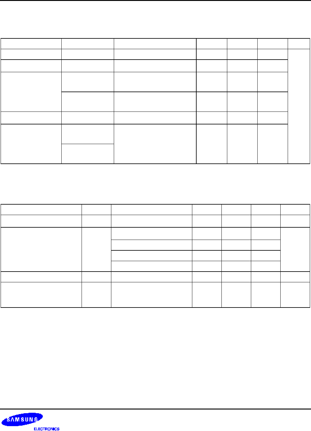
Table 19-8. Voltage Booster Electrical Characteristics
(T
A
= 25 °C, V
DD
= 2.0 V to 5.5 V, V
SS
= 0 V)
Parameter Symbol Test Conditions Min Typ Max Unit
Operating Voltage VDD 2.0 – 5.5 V
Regulated Voltage V
LC0
I
LC0
= 5 uA (1/3 bias) 0.9 1.0 1.15
Booster Voltage V
LC1
Connect 1 MΩ load between
V
SS
and V
LC1
2V
LC0
- 0.1
– 2VLC0
+ 0.1
V
LC2
Connect 1 MΩ load between
V
SS
and V
LC2
3V
LC0
- 0.1
– 3VLC0
+ 0.1
Regulated Voltage V
LC0
I
LC0
= 6 uA (1/2 bias) 1.4 1.5 1.7
Booster Voltage V
LC1
Connect 1 MΩ load between
V
SS
and V
LC1
2V
LC0
- 0.1
– 2VLC0
+ 0.1
V
LC2
Connect 1 MΩ load between
V
SS
and V
LC2
Table 19-9. Characteristics of Voltage Level Detect Circuit
(T
A
= 25
°
C)
Parameter Symbol Conditions Min Typ Max Unit
Operating Voltage of VLD V
DDVLD
1.8 – 5.5 V
Voltage of VLD V
VLD
VLDCON.1.0 = 00b 2.05 2.2 2.35 V
VLDCON.1.0 = 01b 2.25 2.4 2.55
VLDCON.1.0 = 10b 2.8 3.0 3.2
VLDCON.1.0 = 11b 3.7 4.0 4.3
Hysteresys Voltage of VLD ∆V VLCDCON.1-.0=00 – 10 100 mV
Sum of Voltage Booster,
Voltage Detector and Sub-
idle current
IVBVLD IVB+IVLD+IDD4,
VDD=3.0V
– 15 40 uA


