


S3C8245/P8245/C8249/P8249 INSTRUCTION SET
6-17
BAND — Bit AND
BAND dst,src.b
BAND dst.b,src
Operation: dst(0) ← dst(0) AND src(b)
or
dst(b) ← dst(b) AND src(0)
The specified bit of the source (or the destination) is logically ANDed with the zero bit (LSB) of the
destination (or source). The resultant bit is stored in the specified bit of the destination. No other
bits of the destination are affected. The source is unaffected.
Flags: C: Unaffected.
Z: Set if the result is "0"; cleared otherwise.
S: Cleared to "0".
V: Undefined.
D: Unaffected.
H: Unaffected.
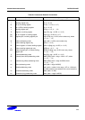
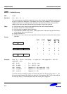
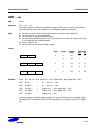
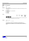
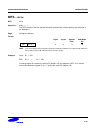
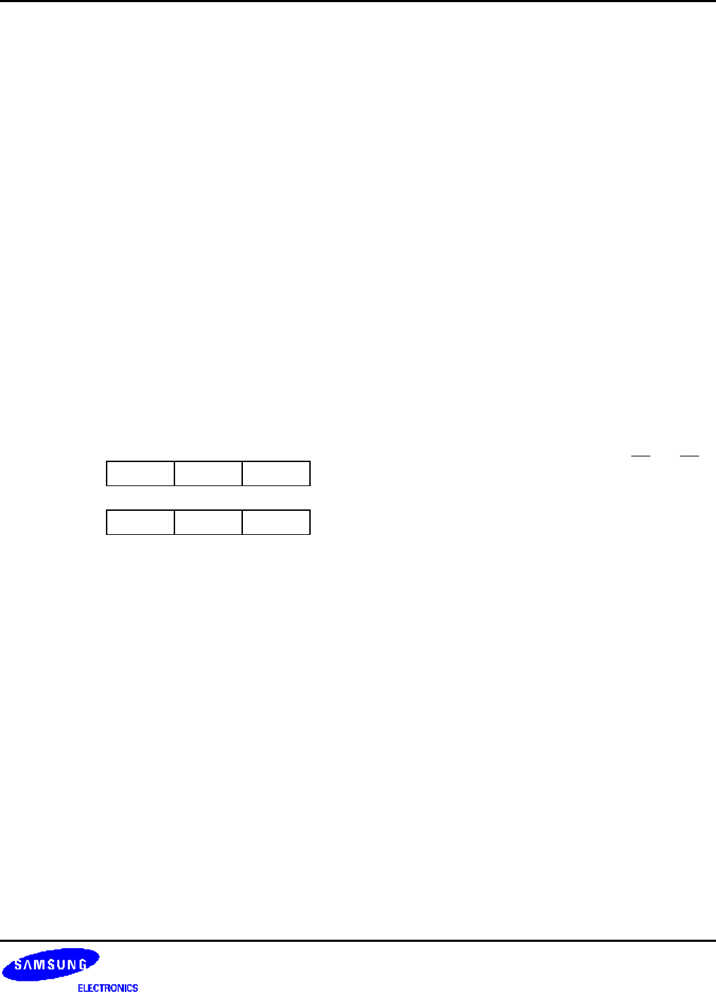
Format:
Bytes Cycles Opcode
(Hex)
Addr Mode
dst src
opc dst | b | 0 src 3 6 67 r0 Rb
opc src | b | 1 dst 3 6 67 Rb r0
NOTE: In the second byte of the 3-byte instruction formats, the destination (or source) address is four
bits, the bit address 'b' is three bits, and the LSB address value is one bit in length.
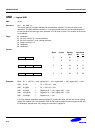
Examples: Given: R1 = 07H and register 01H = 05H:
BAND R1,01H.1 → R1 = 06H, register 01H = 05H
BAND 01H.1,R1 → Register 01H = 05H, R1 = 07H
In the first example, source register 01H contains the value 05H (00000101B) and destination
working register R1 contains 07H (00000111B). The statement "BAND R1,01H.1" ANDs the bit 1
value of the source register ("0") with the bit 0 value of register R1 (destination), leaving the value
06H (00000110B) in register R1.